3 Alignments and Adjustments
3-4
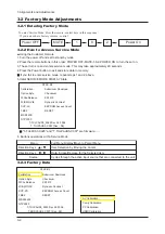
Sharpness
LNA PLUS
UV Dealy
PGA
Calibration Target
CLK_A
CLK_B
Roffset
Goffset
Boffset
BGain
GGain
BGain
H2gain
H4gain
V2gain
V4gain
Sr2gain
Sr4gain
Sl2gain
Sl4gain
Peakth1
Peakth2
Sub_Color
16
4
16
16
2
0
2
0
4
47
60
>>
>>
>>
>>
>>
16
133
68
68
68
294
294
294
Sharpness
LNA PLUS
UV Dealy
PGA
Calibration Target
CLK_A
CLK_B
Roffset
Goffset
Boffset
BGain
GGain
BGain
dB0_Peaking_th1
dB0_Vpeaking_th1
dB1_NoiseAmount
dB1_Peaking_th1
dB1_Vpeaking_th1
dB2_NoiseAmount
dB2_Peaking_th1
dB2_Vpeaking_th2
dB3_NoiseAmount
dB3_Peaking_th1
dB3_Vpeaking_th1
2
4
10
12
12
25
32
32
40
128
80
>>
>>
>>
>>
>>
16
133
68
68
68
294
294
294
NTSC-RF
T-TULPAUS0_0025 Dec 26 2006
T-BRDPAUS5_C007 [Sec : 08]
Calibration
Option Byte
White Balance
W/B MOVIE
SVP-PX
FBE2
MSP4440K
NTP3000
Submicom Download
Checksum
KS1410
Dynamic Contrast
EEPROM Access Count
RESET
Sharpness
LNA PLUS
UV Dealy
PGA
Calibration Target
CLK_A
CLK_B
Roffset
Goffset
Boffset
BGain
GGain
BGain
U Delay
V Delay
255
255
>>
>>
>>
>>
>>
16
133
68
68
68
294
294
294
Summary of Contents for LN-T4065F
Page 17: ...7 Block Diagrams 7 2 7 2 Audio Block Diagram ...
Page 18: ...13 Circuit Descriptions 13 1 13 Circuit Descriptions 13 1 Main Board Block Description ...
Page 19: ...13 Circuit Descriptions 13 2 13 2 Video Signal Path ...
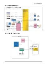
Page 20: ...13 Circuit Descriptions 13 3 13 3 Audio Signal Path 13 3 Side AV Signal Path ...
Page 21: ...13 Circuit Descriptions 13 4 Menu ...
Page 112: ...5 Exploded View Parts List 5 3 M0014 M0013 M0013 T0003 M0215 T0175 5 3 LNT4665F Exploded View ...
Page 118: ...10 Operating Instructions and Installation 10 3 10 3 Remote Control ...
Page 121: ...12 PCB Diagram 12 2 12 2 IP BOARD Diagram 46 ...
Page 125: ...1 Precautions 1 4 Memo ...
Page 131: ...2 Product Specifications 2 6 Memo ...
Page 133: ...14 Reference Infomation 14 2 14 1 2 Supported Mode 1 ...
Page 158: ...4 Troubleshooting 4 3 WAVEFORMS 1 2 PC Input V Sync H Sync 3 LVDS Out CLK ...
Page 166: ...4 Troubleshooting 4 11 WAVEFORMS 6 Tuner CVBS Out Pattern Grey Bar 7 TS DATA Out Clk Data 0 ...
Page 173: ...4 Troubleshooting 4 18 Memo ...
Page 174: ...8 Wiring Diagrams 8 1 8 Wiring Diagram ...
Page 175: ...8 Wiring Diagrams 8 2 Memo ...


