LCD-TV
Chassis : N64D
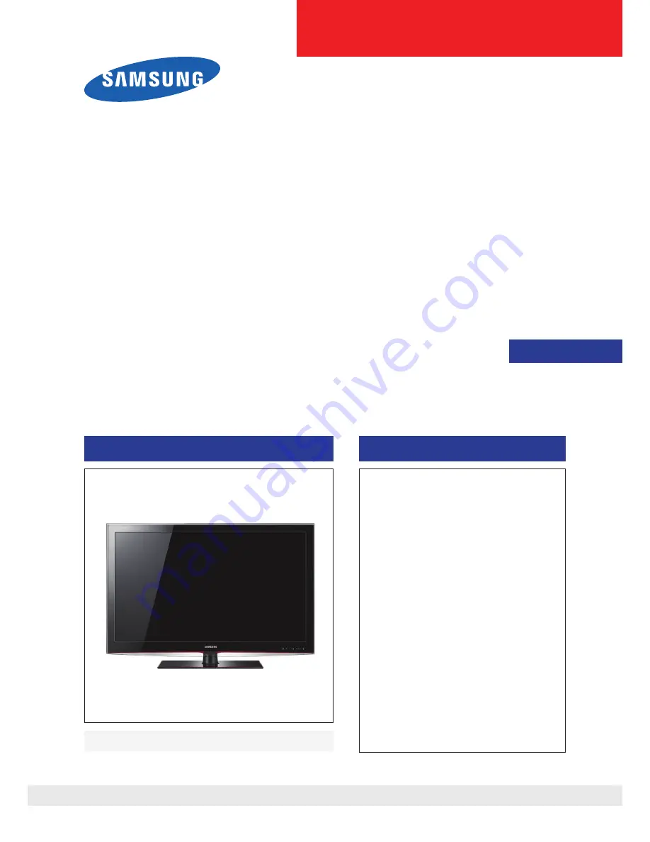
Model
: LN40B550K1H
LN52B550K1H
SERVICE
Manual
TFT-LCD TV
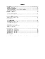
Contents
LN40B550K1
Refer to the service manual in the GSPN (see the rear cover) for the more information.
1. Precautions
2. Product specification
s
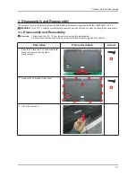
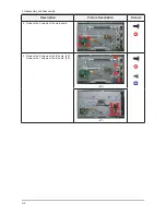
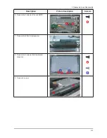
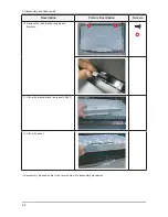
3. Disassembly and Reassembly
4. Troubleshooting
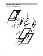
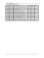
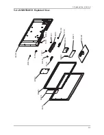
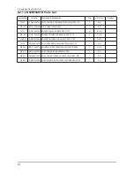
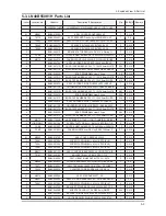
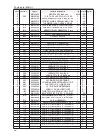
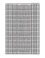
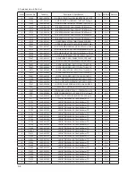
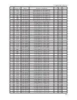
5. Exploded View & Part List
6. Wiring Diagram
Summary of Contents for LN40B550K1H
Page 62: ...4 3 4 Troubleshooting L1 B13V B5V B12V B5V 1 9V B3 3V B9V ...
Page 64: ...4 5 4 Troubleshooting Pin 16 17 Pin 34 35 TP67 TP69 TP71 TP72 TP70 ...
Page 65: ...4 6 4 Troubleshooting WAVEFORMS 1 PC input V sink H sink R G B 2 LVDS output ...
Page 67: ...4 8 4 Troubleshooting Pin 16 17 Pin 34 35 Pin 12 Pin 7 ...
Page 68: ...4 9 4 Troubleshooting WAVEFORMS 3 HDMI input RX_Data RX_Clk 2 LVDS output ...
Page 70: ...4 11 4 Troubleshooting Pin 16 Pin 17 Pin 2 Pin 4 Pin 8 ...
Page 71: ...4 12 4 Troubleshooting WAVEFORMS 4 CVBS OUT Grey Bar 2 LVDS output ...
Page 73: ...4 14 4 Troubleshooting Pin 16 17 Pin 34 35 Pin 2 Pin 4 ...
Page 74: ...4 15 4 Troubleshooting WAVEFORMS 2 LVDS output ...
Page 76: ...4 17 4 Troubleshooting Pin 16 17 Pin 34 35 V3CVBS COMY ...
Page 77: ...4 18 4 Troubleshooting WAVEFORMS 4 CVBS OUT Grey Bar 2 LVDS output ...
Page 79: ...4 20 4 Troubleshooting Pin 16 17 Pin 34 35 COMY COMPB COMPC ...
Page 80: ...4 21 4 Troubleshooting WAVEFORMS 5 Compnent_Y Gray scale Pb Pr Color bar 2 LVDS output ...
Page 82: ...4 23 4 Troubleshooting R416 B12V COMSL COMSR V2SR V2SL TP_L L R R DSL DSR TP_915 TP_916 B3 3V ...
Page 83: ...4 24 4 Troubleshooting WAVEFORMS 6 I2C Data 7 Speaker out ...
Page 119: ...6 6 6 Wiring Diagram Memo ...


