


4-34
4. Troubleshooting
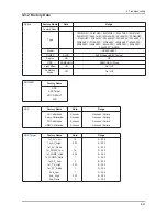
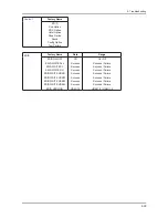
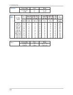
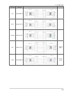
EPA Standard
Factory Name
Data
Range
Std Contr
Std Bright
Std Sharp
Std Color
Std Tint
Std Backlight
95
45
50
50
50
7
0 ~ 100
0 ~ 100
0 ~ 100
0 ~ 100
0 ~ 100
0 ~ 10
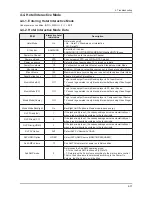
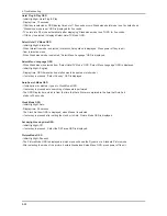
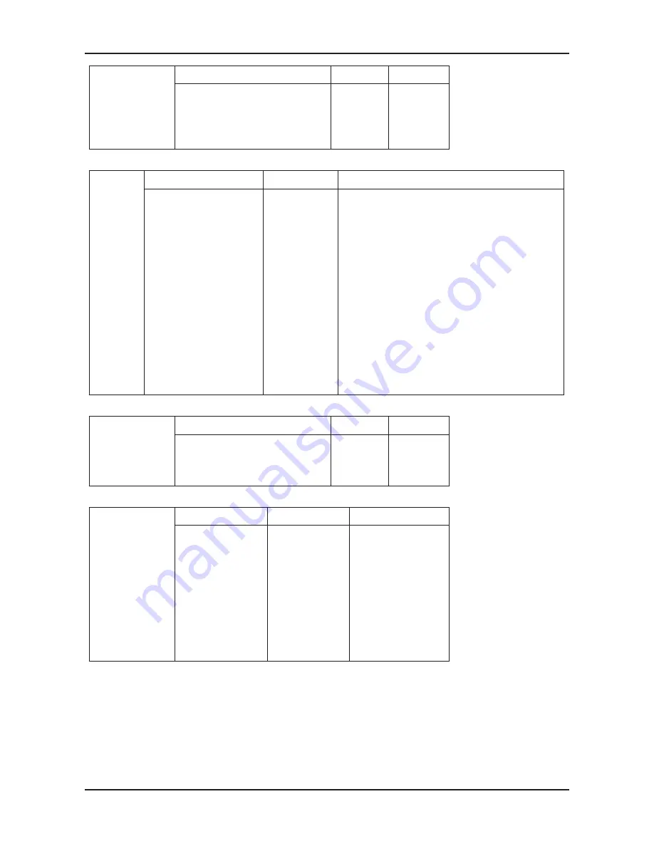
ADJUST
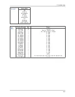
Factory Name
Data
Range
Dynamic Dimming
LNA Plus
Power Key Protect
Uart Select
Debug Mode
Back End Mute
PDP FRC
Visual Test
Standby Mode Time
Delete alt.ver
OTA confirm Time
OTA limit Time
Dynamic CE
FWC
1080p 48Hz
PWM Max
Quick Start
DTV LNA
HDCP Download
Test Pattern
Off
Off
Auto Wall
Debug Off
Disable
45 Min
2 Flash
90 Min
3 Hour
Off
Off
On
100
Auto
On
Off
On / Off
On / Off
Auto Wall / Debug / MDC / On1 / On2
Debug Off / Debug Smart / Debug RunTime
Disable / Enable
2 Min / 45 Min
2 Min / 90 Min
3 Min / 3 Hour
On / Off
On / Off
On / Off
1 ~ 100
Auto / On / Off
On / Off
Off / 1 ~ 13
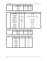
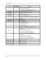
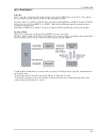
LNA Plus
Factory Name
Data
Range
RF dB1 Level
RF dB2 Level
RF dB3 Level
RF dB4 Level
3
6
12
31
0 ~ 255
0 ~ 255
0 ~ 255
0 ~ 255
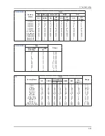
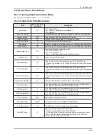
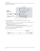
YC_Delay
Factory Name
Data
Range
PAL BG
PAL DK
PAL I
SECAM BG
SECAM DK
SECAM I
NTSC 358
NTSC 443
AV PAL
AV SECAM
AV NT358
AV NT443
AV PAL60
1
1
1
4
4
4
1
1
1
4
1
1
1
0 ~ 3
0 ~ 3
0 ~ 3
0 ~ 7
0 ~ 7
0 ~ 7
0 ~ 3
0 ~ 3
0 ~ 3
0 ~ 7
0 ~ 3
0 ~ 3
0 ~ 3
Summary of Contents for LN40B550K1H
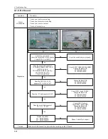
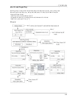
Page 62: ...4 3 4 Troubleshooting L1 B13V B5V B12V B5V 1 9V B3 3V B9V ...
Page 64: ...4 5 4 Troubleshooting Pin 16 17 Pin 34 35 TP67 TP69 TP71 TP72 TP70 ...
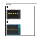
Page 65: ...4 6 4 Troubleshooting WAVEFORMS 1 PC input V sink H sink R G B 2 LVDS output ...
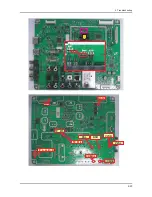
Page 67: ...4 8 4 Troubleshooting Pin 16 17 Pin 34 35 Pin 12 Pin 7 ...
Page 68: ...4 9 4 Troubleshooting WAVEFORMS 3 HDMI input RX_Data RX_Clk 2 LVDS output ...
Page 70: ...4 11 4 Troubleshooting Pin 16 Pin 17 Pin 2 Pin 4 Pin 8 ...
Page 71: ...4 12 4 Troubleshooting WAVEFORMS 4 CVBS OUT Grey Bar 2 LVDS output ...
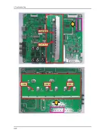
Page 73: ...4 14 4 Troubleshooting Pin 16 17 Pin 34 35 Pin 2 Pin 4 ...
Page 74: ...4 15 4 Troubleshooting WAVEFORMS 2 LVDS output ...
Page 76: ...4 17 4 Troubleshooting Pin 16 17 Pin 34 35 V3CVBS COMY ...
Page 77: ...4 18 4 Troubleshooting WAVEFORMS 4 CVBS OUT Grey Bar 2 LVDS output ...
Page 79: ...4 20 4 Troubleshooting Pin 16 17 Pin 34 35 COMY COMPB COMPC ...
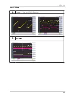
Page 80: ...4 21 4 Troubleshooting WAVEFORMS 5 Compnent_Y Gray scale Pb Pr Color bar 2 LVDS output ...
Page 82: ...4 23 4 Troubleshooting R416 B12V COMSL COMSR V2SR V2SL TP_L L R R DSL DSR TP_915 TP_916 B3 3V ...
Page 83: ...4 24 4 Troubleshooting WAVEFORMS 6 I2C Data 7 Speaker out ...
Page 119: ...6 6 6 Wiring Diagram Memo ...


