1-4
Samsung Electronics
Precaution
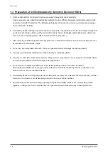
1-3 Precautions for Electrostatically Sensitive Devices (ESDs)
1. Some semiconductor (“solid state”) devices are easily damaged by static electricity.
Such components are called Electrostatically Sensitive Devices (ESDs). Examples include integrated circuits
and some field-effect transistors. The following techniques will reduce the occurrence of component damage
caused by static electricity.
2. Immediately before handling any semiconductor components or assemblies, drain the electrostatic charge from
your body by touching a known earth ground. Alternatively, wear a discharging wrist-strap device. (Be sure to
remove it prior to applying power--this is an electric shock precaution.)
3. After removing an ESD-equipped assembly, place it on a conductive surface such as aluminum foil to prevent
accumulation of electrostatic charge.
4. Do not use freon-propelled chemicals. These can generate electrical charges that damage ESDs.
5. Use only a grounded-tip soldering iron when soldering or unsoldering ESDs.
6. Use only an anti-static solder removal device. Many solder removal devices are not rated as “anti-static” (these
can accumulate sufficient electrical charge to damage ESDs).
7. Do not remove a replacement ESD from its protective package until you are ready to install it.
Most replacement ESDs are packaged with leads that are electrically shorted together by conductive foam,
aluminum foil or other conductive materials.
8. Immediately before removing the protective material from the leads of a replacement ESD, touch the protective
material to the chassis or circuit assembly into which the device will be installed.
9. Minimize body motions when handing unpackaged replacement ESDs. Motions such as brushing clothes
together, or lifting a foot from a carpeted floor can generate enough static electricity to damage an ESD.
Summary of Contents for MAX-G55
Page 24: ...3 12 Samsung Electronics MEMO ...
Page 44: ...5 11 Samsung Electronics MEMO ...
Page 55: ...5 11 Samsung Electronics MEMO ...
Page 57: ...6 2 Samsung Electronics PCB Diagram 6 2 FRONT PCB Top 1 UCW2 USJ1 UCW1 UIC2 ...
Page 59: ...6 4 Samsung Electronics PCB Diagram 6 3 FRONT PCB Bottom FIC1 UIC2 UCW1 USJ1 UCW2 ...
Page 64: ...Samsung Electronics 6 9 PCB Diagram 6 6 SMPS PCB Top CON2 CN1 UB1 CON3 UM1 ...
Page 65: ...6 10 Samsung Electronics PCB Diagram 6 7 SMPS PCB Bottom CON2 CN1 UB1 CON3 UM1 ...
Page 73: ...7 8 Samsung Electronics MEMO ...

