Samsung Electronics
4-4
4-3 CD
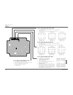
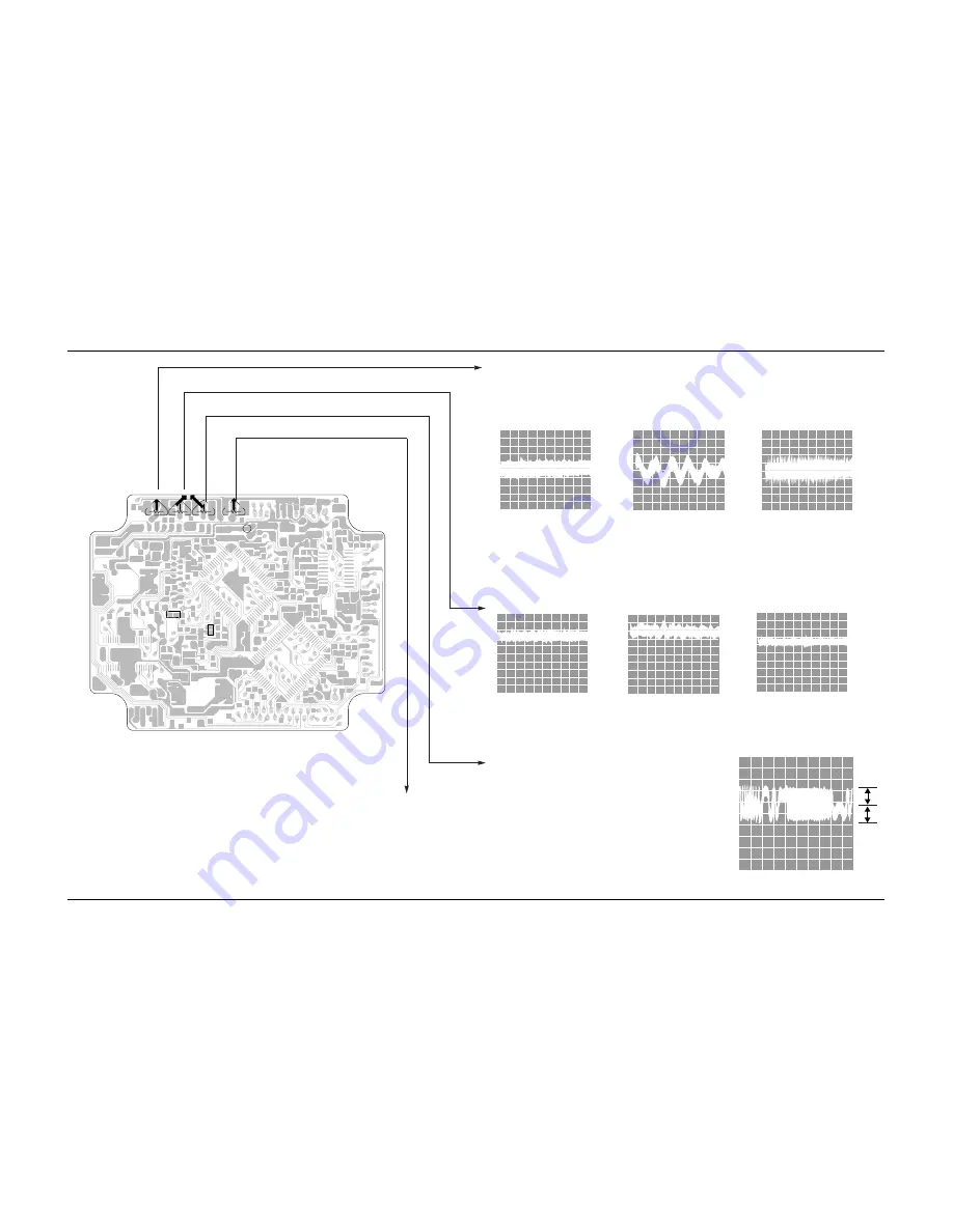
TP2
TP1
Vref
NVR1704 NVR1703 NVR1702
NVR1701
TE CENTER FE CENTER
E.F BAL
F.BIAS
0V
A
B
A=B
---100mV
---0V
---250mV
---0 V
---100mV
---0 V
---0 V
---0 V
---0 V
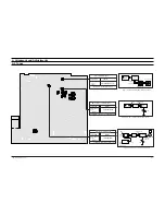
4-3-1 To Adjust FOCUS BIAS(STOP mode)
4-3-3 To Adjust Focus Gain (PLAY mode)
4-3-2 To Adjust Tracking Gain (PLAY mode)
4-3-4 To Adjust E/F Balance (PLAY mode)
1. Set Volt/Div of the oscilloscope to DC 100mV.
2. Ground the scope input and set the waveform to 0V, DC range.
3. Connect the GND terminal of the oscilloscope to
Vref, and (+) terminal to center of TP1.
4. Set NVR1701 to 0mV.
1. Connect the GND terminal of the oscilloscope to Vref and (+) terminal to TP2.
2. Load and play the disc
3. While the disc is running adjust the gain with NVR1704 as shown below.
1. Connect the GND terminal of the oscilloscope to Vref and (+) terminal to TP1.
2. Load and play the disc
3. While the disc is running adjust the gain with NVR1703 as shown in the following figure.
VOLT/DIV : 0.2V
TIME/DIV : 2mS
Normal frequency
Normal frequency
Low frequency
High frequency
Low frequency
High frequency
VOLT/DIV : 0.1V
TIME/DIV : 2mS
VOLT/DIV : 0.1V
TIME/DIV : 2mS
VOLT/DIV : 0.1V
TIME/DIV : 2mS
VOLT/DIV : 0.2V
TIME/DIV : 2mS
VOLT/DIV : 0.2V
TIME/DIV : 2mS
1. Set TIME/DIV of the oscilloscope to 2mS.
2. Set Volt/DIV of the oscilloscope to 0.5V.
3. Ground the scope input and set to DC
and then set the DC range.
4. Connect the GND terminal of the oscilloscope to Vref
and (+) terminal to center to TP2.
5. Load and play the disc.
6. Turn NVR1704 counterclockwise to the minimum value.
7. Raise NVR1702 and adjust the waveform so that its middle
comes to GND of the oscilloscope (or until the upper half
of waveform becomes symmetrical to the bottom half, A=B)
8. Adjust NVR1704 (arrow) for normal sound.
Alignment and Adjustments
Summary of Contents for MM-16
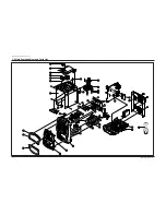
Page 24: ...Samsung Electronics 7 5 Exploded Views and Parts List 7 3 1 CD DECK Exploded View ...
Page 40: ...Block Diagrams KS9282 DSP NIC9282 9 8 Samsung Electronics ...
Page 43: ...10 PCB Diagrams 10 1 Main 10 1 Samsung Electronics ...
Page 44: ...Samsung Electronics 10 2 10 2 Front PCB Diagrams ...
Page 45: ...10 3 Samsung Electronics 10 3 CD 10 3 1 Top View 10 3 2 Bottom View PCB Diagrams ...


