SIGNAL DESCRIPTIONS
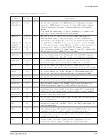
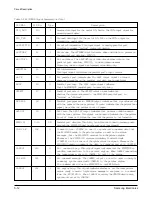
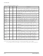
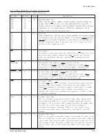
Table 1-1 KS32C6100 Signal Descriptions
S I G N A L
PIN No.
Type
Description
M C L K
206
I
External master clock input. It has a 50% duty cycle and an operating
f
requency up to 33MHz.
CLKSEL
201
I
Clock select. When CLKSEL is “1” (High level), MCLK is used as
internal master clock directly. When CLKSEL is “0” (Low level),
the external MCLK frequency is divided by two and then used as
the internal master clock.
nRSTO
194
O
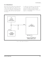
Reset signal output from watch dog timer.
nRESET
195
I
Not reset. nRESET is the global reset input for the KS32C6100.
To reset system, nRESET must be held to Low level
for at least 65 machine cycles.
n B K 0 H W
198
I
Bank 0 data bus width select. When nB0HW is “0”,
the bank 0 data bus is recognized as 16-bit wide.
When nB0HW is “1”, the bank 0 data bus is recognized as 32-bit wide.
T M O D E
197
I
Test pin. For normal operation, this pin should be connected to GND.
T C K
208
I
TA P controller clock.
T M S
204
I
TA P controller mode select.
TDI
202
I
TA P controller data input.
T D O
203
O
TA P controller data output.
TnRST
196
I
TA P controller reset signal.
XA[23:0]/
40~45
I/O
The 24-bit address data bus, XA[23:0], acts as an output
ExtMA[23:0]
47~51
when the ARM core or DMA is accessing the chip-select banks and
54~60
covers the full 16M-word (32-bit) address range of each ROM and
63~68
SRAM bank, and 64K-byte external I/O address range; or it acts as an
input in external master mode and corresponds to ExtMA[23:0],
the lower 24 bits out of 28-bit external master address bus
ExtMA[27:0].
XD[31:0]
75~79
I/O
External bi-directional three-state 32-bit data bus. The KS32C6100 data
81~87
bus supports external 8-bit, 16-bit, and 32-bit bus connection.
89~94
96~102
106~112
nRCS[3:0]
69
O
Not ROM chip select. The KS32C6100 can access up to four external
72~74
ROM banks. nRCS0 corresponds to ROM bank 0, nRCS1 to bank 1,
and so on.
nSCS
28
O
Not RSAM chip select. Selection to access external SRAM bank.
nECS[3:0]
29~32
O
Not external chip select. Four I/O banks are provided for memory-
mapped external I/O operations, each of which contains up to 16K
bytes. The four nECS signals are used to select the four I/O banks
respectively.
n O E
37
O
Not data output enable for ROM/SRAM/External IO.
Whenever a memory access for ROM/SRAM/External IO occurs,
the nOE output controls the output enable port of the specific device.
5-10
Samsung Electronics
Circuit Description
Summary of Contents for MSYS 5150
Page 9: ...2 6 Samsung Electronics Specification Memo ...
Page 16: ...3 26 Samsung Electronics Setup and Installing Memo ...
Page 37: ...4 2 Samsung Electronics Theory of Operation ...
Page 41: ...4 6 Samsung Electronics Memo Theory of Operation ...
Page 116: ...Samsung Electronics 7 9 Maintenance Troubleshooting No Image ...
Page 117: ...Samsung Electronics Maintenance Troubleshooting 7 10 ...
Page 118: ...Samsung Electronics 7 11 Maintenance Troubleshooting All Black ...
Page 119: ...7 12 Samsung Electronics Maintenance Troubleshooting Vertical White Line Band ...
Page 120: ...Samsung Electronics 7 13 Maintenance Troubleshooting Dark Image ...
Page 121: ...7 14 Samsung Electronics Maintenance Troubleshooting Background ...
Page 122: ...Samsung Electronics 7 15 Maintenance Troubleshooting Ghost ...
Page 123: ...7 16 Samsung Electronics Maintenance Troubleshooting Black Dot ...
Page 124: ...Samsung Electronics 7 17 Maintenance Troubleshooting Horizontal Band ...
Page 125: ...7 18 Samsung Electronics Maintenance Troubleshooting Irregular Density ...
Page 126: ...Samsung Electronics 7 19 Maintenance Troubleshooting White Spot ...
Page 127: ...7 20 Samsung Electronics Maintenance Troubleshooting Trembling at the End When OHP Printing ...
Page 128: ...Samsung Electronics 7 21 Maintenance Troubleshooting Poor Fusing Grade ...
Page 132: ...Samsung Electronics 7 25 Maintenance Troubleshooting No Power LCD NO display LED Off ...
Page 133: ...Fuser Error 7 26 Samsung Electronics Maintenance Troubleshooting ...
Page 134: ...Samsung Electronics 7 27 Maintenance Troubleshooting Paper Jam Mis feeding ...
Page 135: ...7 28 Samsung Electronics Maintenance Troubleshooting Paper Jam Jam1 ...
Page 136: ...Samsung Electronics Maintenance Troubleshooting 7 29 Engine Error ...
Page 137: ...7 30 Samsung Electronics Maintenance Troubleshooting Memo ...
Page 187: ...9 28 Samsung Electronics Electrical Parts List ...
Page 189: ...11 Connection Diagram Samsung Electronics 11 1 ...
Page 190: ...12 1 Main Circuit Diagram Samsung Electronics 12 1 12 Schematic Diagrams ...
Page 191: ...Schematic Diagrams 12 2 Samsung Electronics Main Circuit Diagram ...
Page 192: ...Main Circuit Diagram Samsung Electronics 12 3 Schematic Diagrams ...
Page 193: ...Schematic Diagrams 12 4 Samsung Electronics Main Circuit Diagram ...
Page 194: ...Main Circuit Diagram Samsung Electronics 12 5 Schematic Diagrams ...
Page 195: ...Schematic Diagrams 12 6 Samsung Electronics Main Circuit Diagram ...
Page 196: ...Main Circuit Diagram Samsung Electronics 12 7 Schematic Diagrams ...
Page 200: ...12 3 Sensors Circuit Diagram Samsung Electronics 12 11 Schematic Diagrams ...
Page 201: ...Schematic Diagrams 12 12 Samsung Electronics 12 4 Switch Circuit Diagram ...
Page 202: ...Samsung Electronics 12 13 Schematic Diagrams 12 5 Joint Circuit Diagram ...
Page 204: ...Samsung Electronics 12 15 Schematic Diagrams 12 7 PTL Circuit Diagram ...
Page 205: ...Schematic Diagrams 12 16 Samsung Electronics 12 8 SCAN Circuit Diagram ...
Page 206: ...Samsung Electronics 12 17 Schematic Diagrams 12 9 Engin Circuit Diagram ...
Page 207: ...Schematic Diagrams 12 18 Samsung Electronics Engin Circuit Diagram ...
Page 208: ...Samsung Electronics 12 19 Schematic Diagrams 12 10 LIU Circuit Diagram ...
Page 210: ... Samsung Electronics Co Ltd Mar 1999 Printed in Korea P N JC68 00097A Rev 1 00 ELECTRONICS ...


