S I G N A L
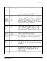
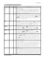
PIN No.
Type
Description
RS4
56
I
Register select bus
RS3
57
These lines are used to address interface memory registers within the
RS2
58
modem. When CS is active, the modem decodes RS0 through RS4 to
RS1
59
address one of its 32 internal interface memory registers. RS4 is the most
RS0
60
significant bit. In a typical design, RS0-RS4 are connected to A0-A4
address lines of the host microprocessor.
D7
8
I/O
Data bus
D6
9
These bi-directional data bus lines provide parallel data transfer between
D5
10
the modem and the host microprocessor. D7 is the most signification bit.
D4
11
The direction of the D0-D7 data bus is controlled by the READ-
φ
2 and
D3
12
WRITE-R/W signals. When not being written into or read from, D0-D7
D2
13
assume the high impedance state.
D1
14
D0
15
CS
54
I
Chip select
The modem is selected and decodes RS0-RS4 when CS becomes active at
which time data transfer between the modem and the host can take
place over the parallel data bus. Typically, CS is driven by address
decode logic.
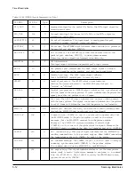
READ-
φ
2
55
I
Read enable (bus mode) or phase2 (6500 bus mode)
If 8085 bus mode is selected (EN85 is connected to ground), this
signal acts as the READ input. If 6500 bus mode is selected (EN85
is pulled-up to +5V), this signal acts as the Phase 2 clock input.
WRITE-R/W
53
I
W rite enable (bus mode) or R/W (6500 bus mode)
If 8085 bus mode is selected (EN85 is connected to ground), this
signal acts as the WRITE input. If 6500 bus mode is selected (EN85
is pulled-up to +5V), this signal acts as the R/W strobe.
IRQ
52
O
Interrupt request
The modem can use IRQ to interrupt the host microprocessor program
execution.IRQ can be enabled in the modem interface memory to be
asserted in response to a specified change of conditions in the modem
status.IRQ is an open drain output and must be connected to an
external pull up resistor of suitable value (typically, a 5.6KW, 1/4 watt,
5% resistor is adequate).
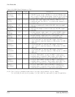
TXDI
79
I
Transmit data input
TXDI is the modem’s transmit data serial input. When configured for
serial data mode (PDME bit is reset) the modem accepts data bits for
transmission via this input. When transmitting data, the modem reads
the TXDI pin on the rising edge of DCLK. When the modem is
configured for parallel data mode (PDME bit is set), the TXID pin is
ignored and transmit data is accepted by the modem via the DBFR
register.
R X D O
95
O
Receive data output
RXDO is the modem receive data output. Received data is output to the
DTE via the RXDO pin in both serial and parallel data modes (PDME bit
set or reset). When receiving data, the modem outputs a data bit on the
falling edge of DCLK. The center of RXDO bits coincides with the rising
edge of DCLK, thus, the DTE should read RXDO on the rising edge of
DCLK.
H A R D WARE INTERFACE SIGNALS DESCRIPTIONS
Table 2-1 Hardware Interface Signal Descriptions
Samsung Electronics
5-19
Circuit Description
Summary of Contents for MSYS 5150
Page 9: ...2 6 Samsung Electronics Specification Memo ...
Page 16: ...3 26 Samsung Electronics Setup and Installing Memo ...
Page 37: ...4 2 Samsung Electronics Theory of Operation ...
Page 41: ...4 6 Samsung Electronics Memo Theory of Operation ...
Page 116: ...Samsung Electronics 7 9 Maintenance Troubleshooting No Image ...
Page 117: ...Samsung Electronics Maintenance Troubleshooting 7 10 ...
Page 118: ...Samsung Electronics 7 11 Maintenance Troubleshooting All Black ...
Page 119: ...7 12 Samsung Electronics Maintenance Troubleshooting Vertical White Line Band ...
Page 120: ...Samsung Electronics 7 13 Maintenance Troubleshooting Dark Image ...
Page 121: ...7 14 Samsung Electronics Maintenance Troubleshooting Background ...
Page 122: ...Samsung Electronics 7 15 Maintenance Troubleshooting Ghost ...
Page 123: ...7 16 Samsung Electronics Maintenance Troubleshooting Black Dot ...
Page 124: ...Samsung Electronics 7 17 Maintenance Troubleshooting Horizontal Band ...
Page 125: ...7 18 Samsung Electronics Maintenance Troubleshooting Irregular Density ...
Page 126: ...Samsung Electronics 7 19 Maintenance Troubleshooting White Spot ...
Page 127: ...7 20 Samsung Electronics Maintenance Troubleshooting Trembling at the End When OHP Printing ...
Page 128: ...Samsung Electronics 7 21 Maintenance Troubleshooting Poor Fusing Grade ...
Page 132: ...Samsung Electronics 7 25 Maintenance Troubleshooting No Power LCD NO display LED Off ...
Page 133: ...Fuser Error 7 26 Samsung Electronics Maintenance Troubleshooting ...
Page 134: ...Samsung Electronics 7 27 Maintenance Troubleshooting Paper Jam Mis feeding ...
Page 135: ...7 28 Samsung Electronics Maintenance Troubleshooting Paper Jam Jam1 ...
Page 136: ...Samsung Electronics Maintenance Troubleshooting 7 29 Engine Error ...
Page 137: ...7 30 Samsung Electronics Maintenance Troubleshooting Memo ...
Page 187: ...9 28 Samsung Electronics Electrical Parts List ...
Page 189: ...11 Connection Diagram Samsung Electronics 11 1 ...
Page 190: ...12 1 Main Circuit Diagram Samsung Electronics 12 1 12 Schematic Diagrams ...
Page 191: ...Schematic Diagrams 12 2 Samsung Electronics Main Circuit Diagram ...
Page 192: ...Main Circuit Diagram Samsung Electronics 12 3 Schematic Diagrams ...
Page 193: ...Schematic Diagrams 12 4 Samsung Electronics Main Circuit Diagram ...
Page 194: ...Main Circuit Diagram Samsung Electronics 12 5 Schematic Diagrams ...
Page 195: ...Schematic Diagrams 12 6 Samsung Electronics Main Circuit Diagram ...
Page 196: ...Main Circuit Diagram Samsung Electronics 12 7 Schematic Diagrams ...
Page 200: ...12 3 Sensors Circuit Diagram Samsung Electronics 12 11 Schematic Diagrams ...
Page 201: ...Schematic Diagrams 12 12 Samsung Electronics 12 4 Switch Circuit Diagram ...
Page 202: ...Samsung Electronics 12 13 Schematic Diagrams 12 5 Joint Circuit Diagram ...
Page 204: ...Samsung Electronics 12 15 Schematic Diagrams 12 7 PTL Circuit Diagram ...
Page 205: ...Schematic Diagrams 12 16 Samsung Electronics 12 8 SCAN Circuit Diagram ...
Page 206: ...Samsung Electronics 12 17 Schematic Diagrams 12 9 Engin Circuit Diagram ...
Page 207: ...Schematic Diagrams 12 18 Samsung Electronics Engin Circuit Diagram ...
Page 208: ...Samsung Electronics 12 19 Schematic Diagrams 12 10 LIU Circuit Diagram ...
Page 210: ... Samsung Electronics Co Ltd Mar 1999 Printed in Korea P N JC68 00097A Rev 1 00 ELECTRONICS ...


