6. Schematic Diagram
6. Schematic Diagram
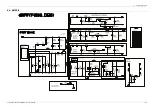
6.1. Overall Block Diagram
D
P- 31 Me cha
F
ro nt
u Co m
D
VD/CD Engine
1
2 8/64MB
DRAM
V
id e o
4 - Da c
A
u dio
De c ode r
PW M
T
I AMP
(6 30)
S
MPS
ES S_P3C (8396)
MPEG Chip
F
M/AM
A
M5 7 6 6
Mo t o r Dr iv e
R
5 F100PGAFB
Front Micom
Re ne s a s
P
T6 3 1 5A
VFD Dr ive r
M
icom
Upda te
F
r o nt End
M
ic AMP
C
VBS (S ca rt)
Y P b P r
V
FD
K
e y
A
UX
D
VD Option
F
u nc tion
In pu t
ADC
U
SB HOST
iP OD o ve r us b
P
OWER
Control
Control
Vide o
8
K- EEPROM
2
M Fla s h
(DVD)
T
une r Control
P
r e AMP
(7 3 0)
F
L
FR
U
S B
C
rys ta l Pr o
IR Amp
(7 30)
A
u dio
De c ode r
/DAC
•
lThe Main Micom IC is R5F100PGAFB. MPEG IC is ES8396SCD.
AMP IC is IRF6645.
•
The Main Micom control each IC in this PCB.
•
Video signal is come from DVD Mecha and go to the MPEG IC.
Then MPEG IC decode this signal to real video signal.
•
Audio signal is come from DVD Mecha, TUNER, AUX, MIC.
Then MPEG IC encode them and sent them to AMP IC.
•
lThis signal go to the Crystal Amplifier (IRF6645). And amplified signal is Low Pass Filtered. This signal is real audio signal.
6-1
Copyright© 1995-2013 SAMSUNG. All rights reserved.
Summary of Contents for MX-F730
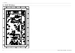
Page 32: ...5 PCB Diagram 5 2 FRONT PCB Top FCN 1 1 5 2 Copyright 1995 2013 SAMSUNG All rights reserved ...
Page 34: ...5 PCB Diagram 5 3 FRONT PCB Bottom 5 4 Copyright 1995 2013 SAMSUNG All rights reserved ...
Page 38: ...5 PCB Diagram 5 5 MAIN PCB Bottom 5 8 Copyright 1995 2013 SAMSUNG All rights reserved ...


