background image

5. PCB Diagram

5. PCB Diagram

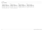
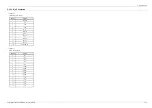
5.1. Wiring Diagram

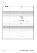
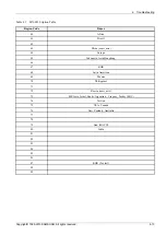
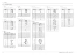
P

in

Signal

Function

Function

Signal

Pin

Pin

Signal

Function

Function

Signal

Pin

Pin

Signal

Function

1

SP+

SP+ 1

1

UART_TX

MICOM Update Signal (Send) 

MICOM Update Signal (Send) 

UART_TX

19

1

DGND

2

SP-

SP- 2

2

UART_RX

MICOM Update Signal (Receive) 

MICOM Update Signal (Receive) 

UART_RX 18

2

DGND

3

SL-

SL- 3

3

DGND

GND

GND

DGND 17

3

DGND

4

SL+

SL+ 4

4

KEY_AD3

Key  Signal 3

Key  Signal 3

KEY_AD3

16

4

JLED9

5

INSW

INSW 5

5

VFD_DO

VFD Data

VFD Data

VFD_DO 15

5

JLEDBL

6

OUTSW

OUTSW 6

6

VFD_CLK

VFD Working Clock Signal

VFD Working Clock Signal

VFD_CLK 14

6

JLEDB

7

GND

GND 7

7

VFD_CE

VFD Enable

VFD Enable

VFD_CE 13

7

JLEDBR

8

D+

D+ 8

8

S

T5V

A

bov/Driver IC Power Supply

Abov/Driver IC Power Supply

M

5.1V 1

2

8

VOL_LED1

9

D-

D-

9

9

S

T5V

R

EMOCON Eye Power Supply

REMOCON Eye Power Supply

S

T5.1V

1

1

9

VOL_LED2

10 REMOCON

REMOCON Eye Signal

REMOCON Eye Signal

REMOCON 10

10

VOL_LED3

11 DGND

GND

GND

DGND 9

11

VOL_LED4

Pin

Signal

Function

Function

Signal

Pin

12 KEY_AD1

Key  Signal 1

Key  Signal 1

KEY_AD1

8

12

VOL_LED5

1

CD_VR

CD_VR 1

13 KEY_AD2

Key  Signal 2

Key  Signal 2

KEY_AD2

7

13

VOL_LED6

2

CD_MPD

CD_MPD

2

14 VOL_UP

Volume Up

Volume Up

VOL_UP

6

14

VOL_DN

3

CD_LD

CD_LD

3

15 VOL_DOWN

Volume Down

Volume Down

VOL_DN

5

15

VOL_UP

4

LD_GND

LD_GND

4

16 DGND

GND

GND

DGND 4

16

L

ED_5.1V

5

SW

SW 5

17 VFD_VP

VFD Driver IC Power Supply

VFD Driver IC Power Supply

VFD_VP

3

17

S

T5.1V

R

EMOCON Eye Power Supply

6

F-

F- 6

18 -VFD

VFD Power Supply(-)

VFD Power Supply(-)

-VFD 2

18

KEY_AD3

7

T-

T-

7

19 +VFD

VFD Power )

VFD Power )

+VFD 1

19

KEY_AD2

8

T+

T+

8

20

REMOCON

9

F+

F+ 9

21

DGND

10 B

B 10

11 C

C 11

12 D

D 12

13 A

A 13

14 E

E 14

Pin

Signal

Function

Function

Signal

Pin

Pin

Signal

Function

15 F

F 15

1

USB1_5V

USB1 Power Supply

USB1 Power Supply

USB1_5V 1

21

DGND

16 VCC

VCC 16

2

USB1_5V

USB1 Power Supply

USB1 Power Supply

USB1_5V 2

20

DGND

17 VREF

VREF 17

3

USB1_DN

USB1 Differential Signal

USB1 Differential Signal

USB1_DN 3

19

DGND

18 GND

GND 18

4

USB1_DN

USB1 Differential Signal

USB1 Differential Signal

USB1_DN 4

18

FLED9

19 DVD_VR

DVD_VR 19

5

USB1_DP

USB1 Differential Signal

USB1 Differential Signal

USB1_DP 5

17

FLEDBL

20 DVD_MPD

DVD_MPD 20

6

USB1_DP

USB1 Differential Signal

USB1 Differential Signal

USB1_DP 6

16

FLEDB

21 DVD_LD

DVD_LD 21

7

USB1_GND

USB1 GND

USB1 GND

USB1_GND 7

15

FLEDBR

22 RF

RF 22

8

USB1_GND

USB1 GND

USB1 GND

USB1_GND 8

14

VOL_LED1

23 V

CC_5V

VCC_5V 2

3

9

USB2_5V

USB2 Power Supply

USB2 Power Supply

USB2_5V 9

13

VOL_LED2

10 USB2_5V

USB2 Power Supply

USB2 Power Supply

USB2_5V 10

12

VOL_LED3

11 USB2_DN

USB2 Differential Signal

USB2 Differential Signal

USB2_DN 11

11

VOL_LED4

Pin

Signal

Function

Function

Signal

Pin

12 USB2_DN

USB2 Differential Signal

USB2 Differential Signal

USB2_DN 12

10

VOL_LED5

1

DGND

GND

GND

DGND 1

13 USB2_DP

USB2 Differential Signal

USB2 Differential Signal

USB2_DP 13

9

VOL_LED6

2

-VP

VFD Driver IC Power Supply

VFD Driver IC Power Supply

-VP

2

14 USB2_DP

USB2 Differential Signal

USB2 Differential Signal

USB2_DP 14

8

VOL_DN

3

-VFD

VFD Power Supply(-)

VFD Power Supply(-)

-VFD

3

15 USB2_GND

USB2 GND

USB2 GND

USB2_GND 15

7

VOL_UP

4

+VFD

VFD Power )

VFD Power )

+VFD 4

16 USB2_GND

USB2 GND

USB2 GND

USB2_GND 16

6

L

ED_5.1V

5

B

-5V

A

MP Power Supply

AMP Power Supply

A

-5V

5

17 AUX_L

AUX1 Left Signal

AUX1 Left Signal

AUX1_L 17

5

S

T5.1V

6

MGND

GND

GND

MGND

6

18 AGND

AUX1 GND

AUX1 GND

AGND 18

4

KEY_AD3

7

P-ON

MICOM Control SMPS Signal

MICOM Control SMPS Signal

P-ON

7

19 AUX_R

AUX1 Right Signal

AUX1 Right Signal

AUX1_R 19

3

KEY_AD2

8

M

+12V

F

AN/SPK LED Power Supply

FAN/SPK LED Power Supply

1

2V 8

20 AGND

GND

GND

AGND 20

2

REMOCON

9

DGND

GND

GND

DGND 9

21 MIC_SIGN

MIC Signal

MIC Signal

MIC_SIGN 21

1

DGND

10 S

T5.5V

A

MP/MICOM/MPEG Power Supply

AMP/MICOM/MPEG Power Supply

S

T5.3V

1

0

22 MIC_SEN

MIC Sensor Signal

MIC Sensor Signal

MIC_SEN 22

11 S

T5.5V

A

MP/MICOM/MPEG Power Supply

AMP/MICOM/MPEG Power Supply

S

T5.3V 1

1

23 AUX_SEN

AUX1 Sensor Signal

AUX1 Sensor Signal

AUX1_SEN 23

12 VARI_SMPS NA

NA

VARI_SMPS 12

Pin

Signal

Function

Function

Signal

Pin

1

-

63V

A

MP GVDD Power(-)

AMP GVDD Power(-)

-

63V 1

2

-

63V

A

MP GVDD Power(-)

AMP GVDD Power(-)

-

63V 2

Pin

Signal

Function

Function

Signal

Pin

3

-

63V

A

MP GVDD Power(-)

AMP GVDD Power(-)

-

63V 3

1

FRLED6

Right Spk LED  Group6 Control Signal

Right Spk LED  Group6 Control SignalL6

1

4

-

63V

A

MP GVDD Power(-)

AMP GVDD Power(-)

-

63V 4

2

FRLED5

Right Spk LED  Group5 Control Signal

Right Spk LED  Group5 Control SignalL5_1

2

5

-

63V

A

MP GVDD Power(-)

AMP GVDD Power(-)

-

63V 5

3

FRLED4

Right Spk LED  Group4 Control Signal

Right Spk LED  Group4 Control SignalL4_1

3

6

SGND

AMP GND

AMP GND

SGND 6

7

SGND

AMP GND

AMP GND

SGND 7

Function

Signal

Pin

8

SGND

AMP GND

AMP GND

SGND 8

4

FRLED3

Right Spk LED  Group3 Control Signal

Right Spk LED  Group3 Control SignalL1

1

9

SGND

AMP GND

AMP GND

SGND 9

5

FRLED2

Right Spk LED  Group2 Control Signal

Right Spk LED  Group2 Control SignalL2

2

10 SGND

AMP GND

AMP GND

SGND 10

6

FRLED1

Right Spk LED  Group1 Control Signal

Right Spk LED  Group1 Control SignalL3

3

11 +

63V

A

MP GVDD Power(+)

AMP GVDD Power(+)

+

63V 1

1

7

F

RM+8V

R

ight Spk LED  Power Supply

Right Spk LED  Power Supply

VCC

4

12 +

63V

A

MP GVDD Power(+)

AMP GVDD Power(+)

+

63V 1

2

13 +

63V

A

MP GVDD Power(+)

AMP GVDD Power(+)

+

63V 1

3

14 +

63V

A

MP GVDD Power(+)

AMP GVDD Power(+)

+

63V 1

4

15 +

63V

A

MP GVDD Power(+)

AMP GVDD Power(+)

+

63V 1

5

Pin

Signal

Function

Function

Signal

Pin

1

FRLED1

Left Spk LED  Group1 Control Signal

Left Spk LED  Group1 Control Signal L6

1

2

FRLED2

Left Spk LED  Group2 Control Signal

Left Spk LED  Group2 Control Signal L5_1

2

Pin

Signal

Function

Function

Signal

Pin

3

FRLED3

Left Spk LED  Group3 Control Signal

Left Spk LED  Group3 Control Signal L4_1

3

1

M5V_PW

BT Power Supply

BT Power Supply

M5V_PW

1

L

B1

2

GND

GND

GND

GND 2

Function

Signal

Pin

3

GND

GND

GND

GND 3

4

FRLED4

Left Spk LED  Group4 Control Signal

Left Spk LED  Group4 Control Signal L1

1

4

BT_RXT

BT Communicate Signal (Receive) 

BT Communicate Signal (Receive) 

BT_RXT

4

5

FRLED5

Left Spk LED  Group5 Control Signal

Left Spk LED  Group5 Control Signal L2

2

5

BT_TXD

BT Communicate Signal (Send) 

BT Communicate Signal (Send) 

BT_TXD

5

6

FRLED6

Left Spk LED  Group6 Control Signal

Left Spk LED  Group6 Control Signal L3

3

6

BT_RST

BT Reset Signal

BT Reset Signal

BT_RST

6

7

F

LM+8V

L

eft Spk LED  Power Supply

Left Spk LED  Power Supply

VCC

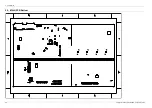
4

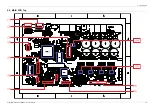
C

NM852

CON13

FLCN1

LB5

RB1

RFCN1

S

M

P

S

C

NM851

SCN1

FCN2

D

e

c

k

Front

VFD

Front

JACK

F

CN4

BTCN1

B

T

(O

p

tio

n

)

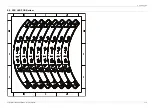
Main

SPK

R

FCN2

UCN1

FCN1

CN1

FCN5

FRCN1

RB5

5-1

Copyright© 1995-2013 SAMSUNG. All rights reserved.

Summary of Contents for MX-F870

Page 1: ...70 ZP SERVICEMANUAL MINI Compact System MX F870 Contents 1 Precaution 2 Product Specification 3 Disassembly and Reassembly 4 Troubleshooting 5 PCB Diagram 6 Schematic Diagram Refer to the service manu...

Page 2: ...ode 4 1 4 1 1 No Power 4 2 4 1 2 No Output 4 3 4 2 Measures to be taken when the Protection Circuit operates 4 7 4 2 1 Operation of Power Block Protection Circuit 4 7 4 2 2 Check AMP in Power Protecti...

Page 3: ...Diagram 6 1 6 2 MAIN 1 6 2 6 3 MAIN 2 6 3 6 4 MAIN 3 6 4 6 5 MAIN 4 6 5 6 6 MAIN 5 6 6 6 6 1 Test Point Wave Form 6 7 6 7 MAIN 6 6 8 6 7 1 Test Point Wave Form 6 9 6 8 MAIN 7 6 10 6 8 1 Test Point Wa...

Page 4: ...h alterations might create a safety hazard Also any design changes or additions will void the manufacturer s warranty 4 Leakage Current Hot Check Figure 1 1 AC Leakage Test WARNING Do not use an isola...

Page 5: ...rect any potential hazards 7 Observe the original lead dress especially near the following areas Antenna wiring sharp edges and especially the AC and high voltage power supplies Always inspect for pin...

Page 6: ...sulation between the blades of the AC plug and accessible conductive parts examples metal panels input terminals and earphone jacks 6 Insulation Checking Procedure Disconnect the power cord from the A...

Page 7: ...not use freon propelled chemicals These can generate electrical charges that damage ESDs 4 Use only a grounded tip soldering iron when soldering or unsoldering ESDs 5 Use only an anti static solder re...

Page 8: ...h x 2 IR Amp Specialized Function Bluetooth Only MX F830B Front Speak LED Lighting CD Ripping Able to ripping while listening New Bass Sound System Called GIGA Sound Twin USB Connectivity USB Host Por...

Page 9: ...IR Amp Specialized Function Front Speak LED Lighting CD Ripping Able to ripping while listening New Bass Sound System Called GIGA Sound Twin USB Connectivity USB Host Portable Audio In 3 5 phi Stereo...

Page 10: ...30 W x 2 IR Amp Specialized Function Front Speak LED Lighting CD Ripping Able to ripping while listening New Bass Sound System Called GIGA Sound Twin USB Connectivity USB Host Portable Audio In 3 5 ph...

Page 11: ...ity 12 dB FM Tuner Total harmonic distortion 0 6 Signal Noise ratio 35 dB Usable sensitivity 70 dB AM Tuner optional Total harmonic distortion 4 Reading Speed 4 8 5 6 m sec CD Disc CD 12 cm Compact Di...

Page 12: ...Total Output Power 1200 Watts MAX 1650 Watts MAX Front speaker output 400 W CH 6 100 Hz 330 W CH 6 100 Hz Rear speaker output Only F870 165 W CH 12 100 Hz Subwoofer 400 W 6 100 Hz 330 W 6 100 Hz Frequ...

Page 13: ...350 W FRONT DISPLAY VFD VFD VFD VFD DIMMER O O O O Bluetooth X MX F830B Only X X X CD DVD CD CD CD CD DVD MP3 O O O O USB HOST O O O O CD RIPPING O O O O TAPE X X X X AUDIO IN O O O O HEADPHONE X X X...

Page 14: ...ssories Item Item code Batteries AAA 4301 000116 TUNER AUX REPEAT GIGA REPEAT A B AUTO CHANGE Remote Control AH59 02554A User s Manual AH68 02606J FM Antenna MX F830B Only FM AM Antenna MX F830 MX F85...

Page 15: ...instructions before performing any work as the IC chips on the PCB are vulnerable to static electricity In order to assemble reverse the order of disassembly Description Description Photo 1 Front Kit...

Page 16: ...mbly and Reassembly Description Description Photo 3 Unplug 2 Cables 4 Front Kitting Assy 5 Front PCB Assy Unfasten 18 Screws and Unplug 1 Cable BH 3 10 WHITE 3 2 Copyright 1995 2013 SAMSUNG All rights...

Page 17: ...3 Disassembly and Reassembly Description Description Photo 6 VFD PCB JACK PCB 7 SMPS PCB Assy Unfasten 2 Screws BH 3 10 BLACK Copyright 1995 2013 SAMSUNG All rights reserved 3 3...

Page 18: ...and Reassembly Description Description Photo 8 Unfasten 3 Screws Unplug 2 wires and power cord BH 3 10 BLACK 9 Unfasten 5 Screws BH 3 10 WHITE 10 SMPS PCB Assy 3 4 Copyright 1995 2013 SAMSUNG All rig...

Page 19: ...ly and Reassembly Description Description Photo 11 MAIN PCB Assy Unfasten 2 Screws BH 3 10 BLACK 12 Unfasten 2 Screws Unplug 2 Cables and the FAN BH 3 10 BLACK Copyright 1995 2013 SAMSUNG All rights r...

Page 20: ...3 Disassembly and Reassembly Description Description Photo 13 Unfasten 4 Screws BH 3 10 SILVER 14 MAIN PCB Assy 3 6 Copyright 1995 2013 SAMSUNG All rights reserved...

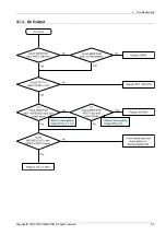
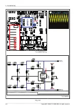
Page 21: ...oting 4 1 Checkpoints by Error Mode Oscilloscope Setting Values Normal Voltage 24 MHz 32 768 KHz Voltage DIV 1 Vol DIV 1 Vol DIV 1 Vol DIV TIME DIV 1 uS DIV 10 ns DIV 0 1 uS DIV Copyright 1995 2013 SA...

Page 22: ...Power Check pattern or replace FVFDV Check VFD Voltage in MAIN PCB CON13 2 4 Check VFD PCB VFD voltag e FVFD 1 2 31 32 Check or replace SMPS Check or replace SMPS Check UIC1 pattern or Replace UIC1 Ch...

Page 23: ...C UIC1 and MPEG IC MIC1 signal Check MAIN PCB ESS IC PIN83 88 89 Replace IRS2053 Replace FET IRF6775 Replace SMPS Check signal input and signal pattern or Replace MAIN PCB Replace UIC1 or MIC1 Yes Yes...

Page 24: ...OMP VS VB VCC IN GND VAA HO CSH OCSET VREF COM DT VSS CSD LO COMP VS VB VCC IN GND VAA 2203 007598 5 6K 4 7K 40N S 8 2K 3 3K 65N S 390 520 220 420KH Z 100V 100NF A 5V_PW 63V UNDEFINED IRS2092ST RPBF 4...

Page 25: ...VB VCC IN GND VAA E B C HO CSH OCSE T VREF COM DT VSS CSD LO COMP VS VB VCC IN GND VAA 2 0CH 2 1C H OPEN 220 420KHZ 390 520 5 6K 4 7K 40NS 8 2K 3 3K 65NS 2203 007598 IRS2092STRPBF 10UF 220NF 100NF 100...

Page 26: ...50V 120PF AC4FL 100NF AC6F AGND AC5F 100NF 10OHM AR5F IN2 VEE OUT2 VCC IN2 IN1 IN1 OUT1 FIL EQ F ILTER TUNER A5V_PW A 5V_PW 1 2KOHM 6 3V 10UF 10UF 6 3V 8 2KOHM 2 7KOHM 27KOHM 1 2KOHM AGND 1 5NF 50V 1...

Page 27: ...he AMP IC Speaker Wire Short 2 If temperature of the AMP IC is over 150 3 There is no power supply for amp Protection Circuit operates when power problem occurs in the SMPS Protection Location Pin No...

Page 28: ...er cord during the test Measurement Resistance using Tester CH MX F830 2CH MX F830B 2CH MX F870 4 2CH MX F850 2 1CH F R CH 2 2 k SUBWOOFER 2 2 k REAR 2 2 k If Measured Resistance is very different fro...

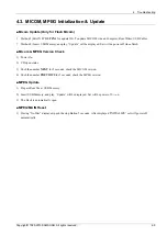
Page 29: ...eck 1 Power On 2 CD open status 3 Push the number NEXT for 5 seconds check the MICOM version 4 Push the number PREVIOUS for 5 seconds check the MPEG version MPEG Update 1 Prepare Rom file at USB Memor...

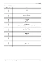
Page 30: ...sert the region code The region code is inserted by the remote control 1 During AUX status MX F870 850 830 830B Push the ENTER button 5 seconds MX F870 850 830 830B 2 When displayed TEST import 46 to...

Page 31: ...ndonesia Asia Hongkong 06 07 KOR 08 Latin American 09 Mexico 10 Philippines 11 12 Russia semi_mic 13 M E Asia Israel Saudi Argentina Uruguay Turkey MIC 14 Taiwan 15 USA Canada 16 New Zealand Australia...

Page 32: ...ndonesia Asia Hongkong 36 37 KOR 38 Latin American 39 Mexico 40 Philippines 41 42 Russia semi_mic 43 M E Asia Israel Saudi Argentina Uruguay Turkey MIC 44 Taiwan 45 USA Canada 46 New Zealand Australia...

Page 33: ...ndonesia Asia Hongkong 66 67 KOR 68 Latin American 69 Mexico 70 Philippines 71 72 Russia semi_mic 73 M E Asia Israel Saudi Argentina Uruguay Turkey MIC 74 Taiwan 75 USA Canada 76 New Zealand Australia...

Page 34: ...Asia Hongkong 96 97 KOR 98 Latin American 99 Mexico 100 Philippines 101 102 Russia semi_mic 103 M E Asia Israel Saudi Argentina Uruguay Turkey MIC 104 Taiwan 105 USA Canada 106 New Zealand Australia 1...

Page 35: ...Asia Hongkong 126 127 KOR 128 Latin American 129 Mexico 130 Philippines 131 132 Russia semi_mic 133 M E Asia Israel Saudi Argentina Uruguay Turkey MIC 134 Taiwan 135 USA Canada 136 New Zealand Austra...

Page 36: ...ply VFD Power Supply VFD 4 16 USB2_GND USB2 GND USB2 GND USB2_GND 16 6 LED_5 1V 5 B 5V AMP Power Supply AMP Power Supply A 5V 5 17 AUX_L AUX1 Left Signal AUX1 Left Signal AUX1_L 17 5 ST5 1V 6 MGND GND...

Page 37: ...MAIN PCB Top MIC1 MIC2 AF IC 1 UIC1 AIC4 AIC3 AIC1 AIC2 FLCN1 FRCN1 R F C N 1 B TC N 1 R F C N 2 USCN1 C N 6 UCN1 SCN1 C O N 1 3 R F IC 1 1 3 4 5 6 7 8 9 2 TP1 TP1 Copyright 1995 2013 SAMSUNG All rig...

Page 38: ...GND 19 DVD_VR 20 DVD_MPD 21 DVD_LD 22 RF 23 VCC_5V 6 RFCN2 Deck Open Close Control Pin No Signal 1 SP 2 SP 3 SL 4 SL 5 INSW 6 OUTSW 7 GND 8 D 9 D 7 USCN1 AUX MIC USB Control Pin No Signal 1 USB1_5V 2...

Page 39: ...5 PCB Diagram 5 2 2 Test Point Wave Form TP1 Copyright 1995 2013 SAMSUNG All rights reserved 5 4...

Page 40: ...5 PCB Diagram 5 3 MAIN PCB Bottom 5 5 Copyright 1995 2013 SAMSUNG All rights reserved...

Page 41: ...5 PCB Diagram 5 4 FRONT JACK PCB Top Copyright 1995 2013 SAMSUNG All rights reserved 5 6...

Page 42: ...5 PCB Diagram 5 5 FRONT JACK PCB Bottom FCN4 F C N 5 1 2 5 7 Copyright 1995 2013 SAMSUNG All rights reserved...

Page 43: ...DP 14 USB2_DP 15 USB2_GND 16 USB2_GND 17 AUX1_L 18 AGND 19 AUX1_R 20 AGND 21 MIC_SIGN 22 MIC_SEN 23 AUX1_SEN 2 FCN4 VOLUME KEY Control Pin No Signal 1 DGND 2 REMOCON 3 KEY_AD2 4 KEY_AD3 5 ST5 1V 6 LED...

Page 44: ...5 PCB Diagram 5 6 FRONT VFD PCB Top FCN2 FCN1 2 1 FIC1 FIC2 5 9 Copyright 1995 2013 SAMSUNG All rights reserved...

Page 45: ...2 M5 1V 13 VFD_CE 14 VFD_CLK 15 VFD_DO 16 KEY_AD3 17 DGND 18 UART_RX 19 UART_TX 2 FCN2 VOLUME KEY Control Pin No Signal 1 DGND 2 DGND 3 DGND 4 JLED9 5 JLEDBL 6 JLEDB 7 JLEDBR 8 VOL_LED1 9 VOL_LED2 10...

Page 46: ...5 PCB Diagram 5 7 FRONT VFD PCB Bottom FIC1 FIC2 5 11 Copyright 1995 2013 SAMSUNG All rights reserved...

Page 47: ...5 PCB Diagram 5 8 SPK LED PCB Top 1 2 3 4 L B 1 R B 1 L B 5 R B 5 Copyright 1995 2013 SAMSUNG All rights reserved 5 12...

Page 48: ...L1 2 L2 3 L3 4 VCC 2 LB5 Front Speaker Led Control Left Pin No Signal 1 L1 2 L2 3 L3 4 VCC 3 RB5 Front Speaker Led Control Rright Pin No Signal 1 L6 2 L5_1 3 L4_1 4 RB1 Front Speaker Led Control Rrigh...

Page 49: ...5 PCB Diagram 5 9 SPK LED PCB Bottom Copyright 1995 2013 SAMSUNG All rights reserved 5 14...

Page 50: ...5 PCB Diagram 5 10 SMPS PCB Top CNM8 5 2 CNM8 5 1 1 2 5 15 Copyright 1995 2013 SAMSUNG All rights reserved...

Page 51: ...ND 2 VP 3 VFD 4 VFD 5 B 5V 6 MGND 7 P ON 8 M 12V 9 DGND 10 ST5 5V 11 ST5 5V 12 VARI_SMPS 2 CNM851 AMP Voltage Supply Pin No Signal 1 63V 2 63V 3 63V 4 63V 5 63V 6 SGND 7 SGND 8 SGND 9 SGND 10 SGND 11...

Page 52: ...5 PCB Diagram 5 11 SMPS PCB Bottom 5 17 Copyright 1995 2013 SAMSUNG All rights reserved...

Page 53: ...LED Driver AUX USB1 FM AM MIC FL SL RL Update DVD CD Engine Tuner Control Key VFD Display Front Led Lighting SPK Led Lighting FR SR RR The Micom IC is R5F100PGAFB 100P MPEG IC is ES8396SCD GSWD same...

Page 54: ...UT ADJ LX EN COM P NC SS FB AGND VI N PGND BST LX VD SGND GND VI N FB ON OFF E B C S D G SGND SGND SGND SGND 63V 63 V 63 V 63 V 63V 63V 63V 63 V 63 V 63 V FROM SM PS MGND SGND DGND DGND VPS P ON A 5V...

Page 55: ...AI N VCC N C RREF VREFC BI ASC B C E RESET RESET VDD GND E B C E B C E B C E B C E B C E B C DGND DGND DGND EQ VFD_CLK VFD_CE VFD_DO KEY_AD3 UARTF_RX UARTF_TX REMOCON VOL_UP KEY_AD1 VOL_DOWN KEY_AD2 S...

Page 56: ...DB 5 DB 6 DB 7 VS33 VD33 CLK DI IO0 VCC HOLD IO3 GND WP IO2 DO IO1 CS SDA VSS WC VCC SCL E2 NC NC FREP BT OPTION BT OPTION SPI_CS FLASH SPI_CS3 EMULATOR SPI EMULATOR OP EN N A OP EN 155 25 141 75 128...

Page 57: ...OTK VOFC VOFC VOSL VOSL VOTR VOTR Vcc1 REV FWD REGO1 VINSL REGO2 TRB_1 VINFC E B C E B C E B C EMULATOR OPTION GND LD_GND GND AGND AGND OPE N DVD ONLY CD ONLY USB2_DP RF B DVD ONLY DVD ONLY CD ONLY SP...

Page 58: ...VCC IN2 IN1 IN1 OUT1 E B C E B C Q3 Q2 Q1 Q0 E B C IN2 VEE OUT2 VCC IN2 IN1 IN1 OUT1 TUR18 0 OHM USE FAN CIRCUIT 27K F870 8 2K 27K 27K 8 2K 8 2K 39K 39K 39K F850 8 2K F830 56K 5 6K 56K 5 6K 27K 8 2K 8...

Page 59: ...6 Schematic Diagram 6 6 1 Test Point Wave Form TP1 Copyright 1995 2013 SAMSUNG All rights reserved 6 7...

Page 60: ...C E B C E B C HO CSH OCSET VREF COM DT VSS CSD LO COMP VS VB VCC IN GND VAA 2CH OMIT 220 420KHZ 390 520 SP EAKER OVER UNDER VOLTAGE PROT ECTION OMIT OMIT 4 2CH 2 1CH AM OMIT USE USE 3716 001316 3716 0...

Page 61: ...6 Schematic Diagram 6 7 1 Test Point Wave Form TP1 Copyright 1995 2013 SAMSUNG All rights reserved 6 9...

Page 62: ...C IN GND VAA E B C E B C HO CSH OCS ET VREF COM DT VSS CSD LO COMP VS VB VCC IN GND VAA 2 0CH 2 1CH OPEN 2 0CH OPEN 220 420KHZ 220 420KHZ 390 520 390 520 5 6K 4 7K 40NS 8 2K 3 3K 65NS 5 6K 4 7K 40NS 8...

Page 63: ...6 Schematic Diagram 6 8 1 Test Point Wave Form TP1 Copyright 1995 2013 SAMSUNG All rights reserved 6 11...

Page 64: ...HVES F_LEDBL 330OHM U2R1 F_LEDBL FR8L VCC_5 1V 1 8W LTL87HVES GND VCC OUT E B C E B C E B C DGND DGND FLED8L FLED9 FLEDBR FLED8 VOL_LED1 DGND VOL_LED4 VOL_LED3 VOL_LED2 USB1_DN USB1_DN VOL_LED5 REM OC...

Page 65: ...GR7 LED3 LED2 LED1 SG10 KS10 SG11 KS11 SG14 KS14 SG15 KS15 SG12 KS12 SG13 KS13 SG9 KS9 SG8 KS8 UARTF_TX VFD_CE DGND VOL_LED1 J LED8 J LEDBL J LED9 VOL_LED3 VOL_LED4 VOL_LED5 VOL_LED6 DGND DGND VOL_LED...

Page 66: ...B C E B C E B C E B C E B C E B C E B C E B C E B C E B C E B C E B C E B C E B C E B C E B C GND SCLK SDATA RESET VCC 120OHM 1 8W 330OHM 1 8 W 50V 100NF DGND UNDEF INED 3857 ST 330OHM 1 8W KSA733 Y D...

Page 67: ...VDD_1 VCC_1 VCC_1 VCC_2 VDD VDD VCC VCC VCC_1 VCC_2 VCC_3 VCC_3 VCC_2 VCC_2 VCC_1 VDD L1 VCC TOTAL 48 EA LEDS L 1 L6_2 L6_2 L1_2 L1_2 L4_2 L5_2 L5_2 2 2 2 2 L4_2 2 2 L3_2 2 2 L3_2 L2_2 L2_2 2 2 2 2 R...

Page 68: ...8 MMSZ5248B ZDM901 MMS Z5248B ZDM901 MMS Z5248B JA3 JA3 VX801S 14D751 VX801S 14D751 RM805 10 1608 RM805 10 1608 RM816 14K 3216 RM816 14K 3216 LB801 0R 20 12 LB801 0R 20 12 RM902 1K 1608 RM902 1K 1608...

Page 69: ...2K 1608 RS953 1K 1608 RS953 1K 1608 RS 803 22 1608 RS 803 22 1608 CS 931 16V 470uF CS 931 16V 470uF RS 913 150K 1608 RS 913 150K 1608 RS 905 100 1608 RS 905 100 1608 RS96 2 1K 1608 RS96 2 1K 1608 RS 9...

Page 70: ...a Japan https gspn2 samsungcsportal com N America S America https gspn3 samsungcsportal com This Service Manual is a property of Samsung Electronics Co Ltd Any unauthorized use of Manual can be punish...

Reviews: