background image

Part Name

Description

Description Photo

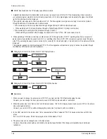
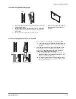
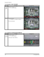
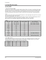
Stand

Remove 4 screws.

: PH,+,WSP,S,M4,L35,ZPC(BLK)

Pull the stand down to remove it from the unit.

: Please lay the PDP unit face down on a soft surface

when removing the stand.

Disassembly & Reassembly

Samsung Electronics

12-1

12. Disassembly & Reassembly

12-1 Overhaul Disassembly & Reassembly 

12-1-1 Separation of ASSY STAND P-BASE   

Notice

- Be sure to separate the power cord before disassembling the unit.
- Discharge the capacitors first when separating PCB's with high capacity capacitors such as SMPS, X Main Board, Y Main 

Board, etc. (A spark may be generated by the electric charge, and there is danger of electronic shock.)

- Check that the cables are properly connected referring to the circuit diagram when disassembling or assembling the unit

taking care not to damage the cables.

- Take care not to cause a flaw in the Glass Filter in the front.
- Assemble the boards in the reverse order of the disassembly.
- The plasma must be layed down on a flat padded surface for disassembly and reassembly.

Part Name

Description

Description Photo

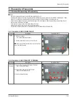
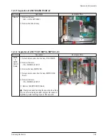
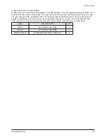
Bracket

Terminal

Remove the 8 screws on the Bracket Terminal.

: BH,+,-,S,M4,L8,ZPC(BLK)

Remove the 2 Hex nuts for the PC input.

: M3,L6,NI PLT,SUM24L,#4-40

Remove Bracket Terminal.

12-1-2 Separation of ASSY BRACKET P-TERMINAL

Summary of Contents for PL42E7SX/RCL

Page 1: ... N_42SD _Spirra Model PL42E7SX RCL PLASMA DISPLAY TV FEATURES DTV Ready PDP TV Supreme Picture Quality Supreme Convenience Quality RF HDMI PC Analog 2 Component 2 Video S Video Slim line design Energy Saving SERVICE Manual PL 42E7S ...

Page 2: ... Manual is a property of Samsung Electronics Co Ltd Any unauthorized use of Manual can be punished under applicable International and or domestic law Samsung Electronics Co Ltd Aug 2006 Printed in Korea AA82 04056A ...

Page 3: ...How to Access Service Mode 3 2 3 3 Factory Data 3 3 3 4 Service Adjustment 3 11 3 5 Software Upgrade 3 14 3 6 Replacements Calibration 3 15 Chapter 4 Exploded View Part List 4 1 PL42E7SX RCL 4 1 Chapter 5 Electrical Part List 5 1 PL42E7SX RCL Service Item 5 1 Chapter 6 Troubleshooting 6 1 First Checklist for Troubleshooting 6 1 6 2 Checkpoints by Error Mode 6 2 6 3 Troubleshooting Procedures by AS...

Page 4: ...apter 11 Operation Instruction Installation 11 1 Product Features and Functions 11 1 11 2 Installation Notes and Precautions 11 5 Chapter 12 Disassembly Reassembly 12 1 Overhaul Disassembly Reassembly 12 1 Chapter 13 Circuit Description 13 1 Power ON OFF Signal Timing Sequence 13 1 13 2 Partial Block Description 13 2 Chapter 14 Reference Information 14 1 Other issues related to other products 14 1...

Page 5: ...V user receives HD rated broadcasts The digital distributed TV Ready Technique can render HD sources as HD rated However you need to install a set top box for this purpose The digital TV alone cannot render HD broadcasting as HD rated Install the formal set top box for HD broadcasts When a digital distributed TV user selects normal size 4 3 to receive SD rated digita broadcasts The digitally distr...

Page 6: ...e console through a wide TV by selecting the aspect ratio to normal 4 3 or wide 21 9 the left and right or top and bottom of the picture will not be displayed This symptom appears in other manufacturer s TV s The three appliance companies are trying to resolve the problem through the Ministry of Information and Communication Changing the Order of the Picture Size for 16 9 Display Devices Changing ...

Page 7: ...ng is a television broadcasting signal digitized and transmitted according to the United States terrestrial digital broadcast standard or ATSC Mono A type of audio interface that transmits the audio signal through a single channel only Through a mono interface it is hard to experience stereophonic sound and the sound is played using only one speaker Reception Sensitivity Amplification LNA A signal...

Page 8: ...ismatch on the TV Progressive Scan Progressive scan displays the entire frame in a single sweep so as to provide clearer and sharper visual quality DVD Digital Versatile Disc DVD is a large capacity storage media that can store multime dia content such as video games audio applications etc using MPEG 2 video compression technology on a CD sized disc DRC This is a sound quality enhancement function...

Page 9: ...hree primary colors of light R G and B the number of possible colors for a pixel is 256 x 256 x 256 16 777 216 or 16 7 million colors If 12 bits are used for a pixel the gradation is 212 or 4096 for a color Since three colors R G and B are used 4096 x 4096 x 4096 or 68 7 billion colors are support ed per pixel Since 68 7 billion colors are far more than 16 7 million colors the picture will be disp...

Page 10: ...a of the signal broadcast from a broadcast station is smaller than that of possible color coordinates Moreover a TV provides a smaller color coordinate area than that of the signal from the broadcasting station even though the size of the color coordinate area varies depending on the TV model In general Color Reproductivity is used as follows The Color reproductivity of a TV is a certain of NTSC T...

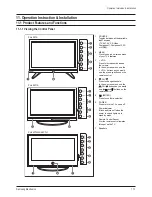
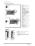
Page 11: ...ss to increase or decrease the volume In the on screen menu use the VOL buttons as you would use the and buttons on the remote control 4 CH Press to change channels In the on screen menu use the CH buttons as you would use the and buttons on the remote control 5 ENTER Press to confirm a selection 6 POWER Press to turn the TV on and off Power Indicator Blinks and turns off when the power is on and ...

Page 12: ...k of an external device 5 AUDIO OUT Audio outputs for external devices 6 ANT IN 75Ω Coaxial connector for Air Cable Network 7 COMPONENT IN 1 2 Video Y PB PR and audio L AUDIO R component inputs 8 PC IN Connect to the video output jack on your PC 9 PC AUDIO IN Connect to the audio output jack on your PC 10 AUDIO L R AV IN 1 Audio inputs for external devices such as a camcorder or VCR 11 VIDEO AV IN...

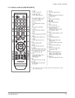
Page 13: ...P broadcast 15 SRS Selects SRS TruSurround XT mode 16 SOURCE Press to display all of the available video sources 17 PRE CH Tunes to the previous channel 18 SLEEP Press to select a preset time interval for automatic shut off 19 PC Selects the PC mode directly 20 CH Press to change channels 21 EXIT Press to exit the menu 22 UP DOWN LEFT RIGHT ENTER Use to select on screen menu items and change menu ...

Page 14: ... DVD or Set Top Box 18 TV DVD STB CABLE VCR Press to operate your TV DVD STB CABLE box or VCR 19 SOURCE Press to display all of the available video sources 20 PRE CH Tunes to the previous channel 21 SLEEP Press to select a preset time interval for automatic shut off 22 PC Selects the PC mode directly 23 CH Press to change channels 24 EXIT Press to exit the menu 25 UP DOWN LEFT RIGHT ENTER Use to s...

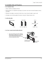
Page 15: ...led on plaster or wood 4 The package contents and parts supplied for the wall mount are subject to change without prior notice 11 2 2 Mounting Kits Wall Mount Bracket Plastic Hanger 4 EA SCREW 4 EA ASSY HINGE Screws 1EA LEFT 1EA RIGHT 1EA Captive Screws Wall Mount Bracket ASSY HINGE RIGHT Separate ASSY HINGE into Left and Right ASSY HINGE LEFT 1 The wall mount bracket is delivered separately Pleas...

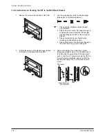
Page 16: ...r fingers while installing and adjusting the angle 4 Please tightly secure the wall mount bracket to the wall to avoid injury from a falling SET 3 Tighten the screws of the plastic hanger shown in picture 2 to the back side of the PDP 4 Remove the Safety Pins Fasten the 4 plastic latches assembled at step on the back side of the PDP using the guide holes of the wall mount push and hook down to sec...

Page 17: ...afety pins underneath the PDP If the safety pins are not removed the angle cannot be adjusted Any attempt to do so may cause damage to the PDP 2 Hold onto the bottom of the PDP and pull forward fully as directed by the arrow as illustrated to adjust the angle 0 20 by 2 Insert the Safety Pins to the front guide holes on both sides as illustrated in figure Viewing the PDP after connecting the extern...

Page 18: ...11 8 Samsung Electronics MEMO ...

Page 19: ...in Board Y Main Board etc A spark may be generated by the electric charge and there is danger of electronic shock Check that the cables are properly connected referring to the circuit diagram when disassembling or assembling the unit taking care not to damage the cables Take care not to cause a flaw in the Glass Filter in the front Assemble the boards in the reverse order of the disassembly The pl...

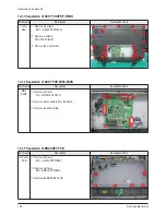
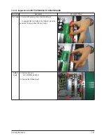
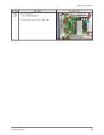
Page 20: ...16 ZPC BLK Remove the Cover Rear 12 1 4 Separation of ASSY PCB MISC MAIN Part Name Description Description Photo Main Board Remove 4 screws PH WWP M3 L8 NI PLT Remove all connectors from the board Remove the Main Board 12 1 5 Separation of BRACKET PCB Part Name Description Description Photo Bracket PCB Remove 4 screws BH S M4 L8 ZPC BLK Remove 2 screws BH B M4 L8 ZPC BLK Remove the BRACKET PCB ...

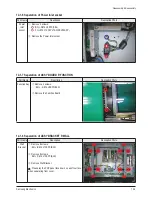
Page 21: ...et socket 12 1 7 Separation of ASSY BOARD P FUNCTION Part Name Description Description Photo Function Key Remove 2 screws BH S M4 L8 ZPC BLK Remove the Function Board 12 1 8 Separation of ASSY BRACKET P WALL Part Name Description Description Photo Wall Bracket Remove 8 screws BH B M4 L12 ZPC BLK Remove 8 screws BH S M4 L10 ZPC BLK Remove Wall Bracket Please lay the PDP panel face down on a soft su...

Page 22: ...Remove 11 screws BH S M4 L8 ZPC BLK Speaker Remove 4 screws BH WP B M4 0 L12 ZPC BLK SWRCH18A Remove the Speaker 12 1 9 Separation of ASSY SPEAKER P Part Name Description Description Photo Power IR Board Remove 2 screws BH S M4 L8 ZPC BLK Remove the Power IR Board 12 1 10 Separation of ASSY BOARD P POWER IR ...

Page 23: ...3 L8 NI PLT Remove the SMPS DC DC Board Wear gloves when handling the power board as there may be some remaining electrical charge in the capacitor Specifically avoid touching any part of the capacitor Disassembly Reassembly Samsung Electronics 12 5 Part Name Description Description Photo Side AV Remove 2 screws BH S M4 L8 ZPC BLK Remove the Side AV assy 12 1 11 Separation of ASSY BOARD P SIDE AV ...

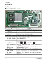
Page 24: ...DULE P LOGIC MAIN BOARD Part Name Description Description Photo Logic Board Detach all connectors from the Logic Main Board Remove 4 screws WSP PH M3 L8 NI PLT Remove the Logic Main Board Disassembly Reassembly 12 6 Samsung Electronics ...

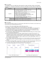
Page 25: ...IN BOARD Part Name Description Description Photo Flat Cable Detach all Connectors from the X Main Board To separate the Flat Cable of the X Board press the upper and the lower sides of the connector X Main Board Remove 4 screws PH WWP M3 L8 NI PLT Remove the X Main Board ...

Page 26: ...Name Description Description Photo Flat Cable Detach the 4 scan board connectors from the panel by pulling the holder from both the top and bottom ends Y Scan Remove 2 screws PH WWP M3 L8 NI PLT Connectors Separate the scan board from the Y Main Board by detaching the 3 connectors and remove the Scan Boards ...

Page 27: ...Disassembly Reassembly Samsung Electronics 12 9 Part Name Description Description Photo Y Main Board Remove 4 screws PH WWP M3 L8 NI PLT Detach all connectors from the Y Main Board ...

Page 28: ...WWP M3 L8 NI PLT Remove the still bar Buffer Detach the all connectors from the buffer board Remove 10 screws PH WWP M3 L8 NI PLT Remove the E Board and F Board Disassembly Reassembly 12 10 Samsung Electronics 12 1 16 Separation of ASSY PDP MODULE P ADDRESS BUFFER BOARD ...

Page 29: ...UTPUTS Va Vg vs 3 4V turn off sequence Vca Vcs Keep Display ON w o display flicker while 3cycle full dip condition Standby step turn off for µ processor reset µ 1 When connecting the AC power cord Stand By 5V from the Main SMPS is supplied to the Main Board Pin 3 of CN1002 of Main Board 2 When pressing the Power button on the remote control or on the main body PS_ON Pin 5 of CN1002 of Main Board c...

Page 30: ...peak loading at 90V AC The power supply shall automatically recover from AC power loss Note that nominal voltages for test purposes are considered to be with 1 0V of nominal STD_5V Vpr2 3 3V is a SELV standby voltage that is always present when AC mains voltage present 3 Output Over Voltage Protection The over voltage sense circuitry and reference shall reside in package that are separate and dist...

Page 31: ...er supply The power supply shall either shutdown and latch off for shorting is removed the P S shall recover The power supply shall be capable of withstanding a continuous short circuit to the output without damage or over stress to the unit components PCB traces connectors etc under the input conditions specified in Section 3 above Current Protection as defined below Output Over Current Limit Uni...

Page 32: ...COM Initial image option PIN Initial image select F W or BLACK Jumper Yes or Full White Jumper No Black Micom Loading 5Pin Connector or Uart Connector The connector to load the Micom drive program The program is loaded by connecting to the GA WRITER Connector that loads and controls 512K data and connects kiss can Board ARM PROCESSOR IC block Control signal to drive logic main Buffer Connector The...

Page 33: ...ly displayed Therefore you have to conduct a short test for each part If the Vref voltage Voltage Divider Voltage is lower than 1 25V check the resistance of the resistance output part and check if the circuit status is normal This applies the voltage and the proper Vref voltage and results in the screen being properly displayed If the screen is abnormally displayed even though the Vref voltage is...

Page 34: ...d That is the pixel whose wall charge has been formed by the Address Discharge forms a Sustain Discharge vis the following Sustain pulse 2 Sustain Discharge A Sustain Discharge is a Self Sustaining Discharge formed by the accumulation of the electric potential of the Sustain pulse gen erally 200 210 Volt alternating over the X and Y electrodes during the sustain period and the wall charge dependin...

Page 35: ...e function of each board 1 X Drive Board This is connected to the X port part of the panel 1 Sustain voltage waveform including ERC is output and 2 Ve bias in the Scan section is maintained 2 Y Drive Board This is connected to the Y port part of the panel It outputs 1 Sustain voltage wave form including ERC and 2 Y Rising Falling Ramp waveform and maintains 3 Vscan bias 3 Y Buffer Board A board wh...

Page 36: ...FPC output electrodes sequentially one line at a time At this time Vscan is called the Scan Bias Voltage A Vscan voltage of approximately 175 Volt Vsc_1 is supplied to the electrode lines For the other lines 56 volt Vsc_h is higher than Vscan l by 120V is supplied However negative wall charges are accumulated on the Y electrode by the Ramp pulse and positive wall charges are accumulated on the add...

Page 37: ...nce 0 2 When no signal is output to the gate GND FET changes to an open circuit i e an insulator of resistance High Voltage Switching of the FET Operation 1 When no signal is applied to G1 FET1 is opened and when the signal is applied to G2 FET2 short circuits GND is output via the output terminal 2 When a signal is applied to G1 FET1 short cir cuits and when no signal is applied to G2 FET2 is ope...

Page 38: ...iption 13 10 Samsung Electronics Drive Board Connector Layout 1 X Main Board 1 Vs 2 Vs 3 DGND 4 DGND 5 Ve 6 DGND 7 DGND 8 Vcc CN4003 Signal 140mm 240mm 8 1 CN4004 15 Pin Connector X FPC Connector Power CN4001 CN4000 ...

Page 39: ...lectronics 13 11 2 Y Main Board CN5401 Panel CN5402 Panel CN5503 Panel CN5502 Panel CN5000 Panel 280mm CN5001 signal 1 9 CN5005 CN5403 CN5010 174mm CN5400 CN5003 CN5404 CN5004 9 Vs 8 Vs 7 GND 6 GND 5 Vset 4 GND 3 Vscan 2 GND 1 Vcc ...

Page 40: ...ions Y Main 120usec 70usec Falling ramp Variable register Rising ramp Variable register Vset Vs Vsc_l Vsc_h Ve Va 201V 207V 190V 120V 110V 65V Adjust the drive waveform so that the main reset rising falling 40usec is the same as those in the F W pattern Attachment 1 reference ...

Page 41: ...Circuit Description Samsung Electronics 13 13 Check that the output of X Out of the X board follows the waveform of Attachment 2 when the power is supplied X OUT ...

Page 42: ...Circuit Description 13 14 Samsung Electronics Attachment 1 Y Output Waveform Rising Ramp Falling Ramp Rising Ramp Falling Ramp ...

Page 43: ...Circuit Description Samsung Electronics 13 15 Scan_l Even_Scan Y Sustain ...

Page 44: ...Circuit Description 13 16 Samsung Electronics Attachment 2 X Output Waveform X Sustain ...

Page 45: ... 3D digital comb video decoder that supports NTSC PAL and SECAM a HDTV sync separator motion adaptive de interlacing engine and the video format conversion engine supporting multi window display in many different output modes M30840SGP IC MICOM With a 16 Mbyte address space this microcomputer combines advanced instruction manipulation capabilities to process complex instructions by less bytes and ...

Page 46: ...ard Pin No Signal 1 6 5V 2 RTN 3 12V 4 RTN 5 18Vamp 6 18Vamp 7 RTN_amp 8 RTN_amp 9 Vt 10 RTN CN2013 Logic B D CN902 Main Board Pin No Signal Pin No Signal Pin No Signal 1 GND 12 TXOUT2 23 TXOUT0B 2 GND 13 GND 24 TXOUT0B 3 TXOUT 14 GND 25 4 TXOUT 15 TXOUTCLK 26 GND 5 GND 16 TXCLKOUT 27 SCL_G 6 GND 17 28 GND 7 TXOUT 18 29 SDA_G 8 TXOUT 19 TXOUT3 30 GND 9 20 TXOUT3 31 10 21 32 GND 11 TXOUT2 22 33 GND...

Page 47: ... Board CN001 Power Button Pin No Signal 1 GND 2 LED 3 ST5V 4 GND 5 KEY_INPUT2 6 7 8 IR_7414 CN501 Main Board Speaker Out Pin No Signal 1 SPK_R 2 SPK_R 3 SPK_L 4 SPK_L CN741 Main Board CN1 Function Board Pin No Signal 1 KEY_INPUT1 2 KEY_INPUT2 3 GND ...

Page 48: ...that senses the quantity of light It senses the illumination and automatically adjusts the screen brightness according to the surrounding brightness when the Power Saving Mode of the User menu is set to Auto No Loc No Description CN102 S VIDEO2 Input Jack CN103 AV2 Input Jack CN104 Earphone Jack CN105 Side AV Connector 9 2 Power IR Board 9 3 Function Board 9 4 Side AV Board ...

Page 49: ...N 6 RTN 7 12V 8 PS_ON 9 RTN 10 STBY 11 FAN_ON 12 FAN_D CN803 Main SMPS CN101 Main Board Pin No Signal 1 6 5V 2 RTN 3 12V 4 RTN 5 18Vamp 6 18Vamp 7 RTN_amp 8 RTN_amp 9 Vt 10 RTN CN810 Main SMPS CN2013 Logic Board Pin No Signal 1 STBY 2 VS_ON 3 N C 4 PS_ON 5 RTN 6 5 3V 7 RTN 8 RTN 9 5 3V 10 5 3V CN809 Main SMPS CN3 DC DC SMPS Pin No Signal 1 5 3V 2 Vg 3 RTN 4 RTN 5 RTN 6 RTN 7 RTN 8 Va 9 Va 10 N C 1...

Page 50: ...RTN 5 RTN 6 RTN 7 RTN 8 Va 9 Va 10 N C 11 Vs 12 Vs CN5 DC DC SMPS CN2710 F Buffer Pin No Signal 1 RTN 2 N C 3 D5 3V 4 N C 5 Va CN2 DC DC SMPS CN5010 Y B D Pin No Signal 1 Vs 2 Vs 3 RTN 4 RTN 5 Vset 6 RTN 7 Vscan 8 RTN 9 Vg 10 D5 3V CN4 DC DC SMPS CN4004 X B D Pin No Signal 1 Vs 2 Vs 3 RTN 4 RTN 5 Ve 6 RTN 7 RTN 8 Vg 9 D5 3V ...

Page 51: ...P LOGIC MAIN BOARD BN96 03106A Logic Main Board ASSY PDP MODULE P X MAIN BOARD BN96 03101A X Drive Board ASSY PDP MODULE P Y MAIN BOARD BN96 03102A Y Drive Board ASSY PDP MODULE P Y MAIN SCAN BUFFER BN96 03103A Y Buffer Board ASSY PDP MODULE P ADDRESS E BUFFER BN96 03104A Address Buffer Board ASSY PDP MODULE P ADDRESS F BUFFER BN96 03105A Address Buffer Board ...

Page 52: ...9 8 Samsung Electronics MEMO ...

Page 53: ...T V 6 1 F n 0 0 1 3 5 1 C V 6 1 F u 0 0 1 2 5 1 C 1 0 1 D V 6 1 F u 0 0 1 7 4 1 C R104 100Kohm V 5 2 F n 0 0 1 1 3 1 C 3 1 1 D B 4 1 1 C V 0 5 F n 0 0 1 T 5 1 0 L 2 1 0 2 B C A 1 0 1 D B T J 1 2 1 2 3 5 4 H 1 H H 6 1 1 P T 9 0 1 D B 5 1 1 P T 1 J D A T U O V 2 3 N I V M _ D V 3 3 B 0 2 1 P T F n 0 0 1 V 5 B A 5 2 D 7 1 1 1 P A 4 0 1 C I 8 0 1 C 6 2 1 C 1uF C141 10V F n 0 0 1 F n 0 0 1 3 2 1 C 1 1 ...

Page 54: ...L C S 1 K L C S 6 1 D D V 1 S S V 7 8 T U O X 9 N I X 37 P3 5 PWM5 2 P3 6 PWM6 2 38 NC 39 4 2 0 A D S 1 T A D S 40 P1 4 VSYNC O P1 5 HSYNC O 41 P1 6 CLAMP O 42 43 1 T N I 1 0 P 3 0 3 6 2 P 7 2 P 1 3 2 3 0 M W P 0 3 P 3 3 1 M W P 1 3 P 34 P3 2 PWM2 SCL1 2 35 P3 3 PWM3 SDA1 2 P3 4 PWM4 2 36 22 VSS2 3 2 3 D A 3 1 P 0 2 P 4 2 1 2 P 5 2 6 2 2 2 P 7 2 3 2 P 8 2 4 2 P 5 2 P 9 2 15 P0 5 2 P0 6 2 16 NC 17 ...

Page 55: ... 6 1 C S K 1 0 3 Q 6 2 3 R m h o K 0 1 6 0 0 1 U 1 0ohm R396 1 H T G 0 3 C 3 S D C 9 4 3 D 8 5 3 P T 9 7 3 P T 1 m h o 5 7 1 5 3 R W 0 1 1 m h o 0 0 1 6 0 4 R 1 m h o K 8 1 2 4 3 R H T G 0 3 C 3 S D C 8 5 3 D 1 7 3 P T 1 2 0 1 U 1 C C V _ C D D 4 1 0 1 U 1 F E R X m h o 0 7 4 F p 0 0 1 2 3 3 C m h o 0 3 0 4 R W 0 1 1 8 3 3 R 1 L C S _ C P 1 F E R X F E R X F E R X V 5 A 8 1 0 1 U 5 3 3 R m h o 0 3...

Page 56: ...1 3 4 4 P T 1 2 3 4 D 1 1 3 4 D 1 2 3 2 3 4 P T 1 1 4 4 D 1 2 3 W 0 1 1 2 2 0 1 U 1 m h o K 7 4 1 5 4 R 0 2 4 D 0 3 4 R m h o K 0 1 m h o 0 1 4 6 4 R 6 6 4 R m h o 0 1 1 6 4 R m h o 0 1 m h o 6 5 8 3 4 R W 0 1 1 8 3 4 D E S 8 4 1 4 D B M M 1 2 3 5 4 4 D 1 2 3 m h o 0 7 4 4 4 4 R 0 3 4 P T 1 V 5 A m h o K 0 1 1 3 4 R 1 4 4 4 P T 1 0 4 4 P T 1 1 4 4 P T 2 4 4 P T 1 0 3 4 D B 2 6 Z L R V 6 1 1 0 4 C ...

Page 57: ...G I S C C V 6 3 B 2 C C V 4 C N 5 B 2 D N G 6 7 A 2 D N G A 2 C C V 8 A 2 T U O 9 A D N G 9 2 A D D V 3 B 2 T U O 0 3 I D S I K C R L 1 3 2 3 I K C I V D N G 3 3 4 3 D D V 5 3 1 2 G I F N O C T E S E R 2 2 L C S 3 2 4 2 A D S S E R 5 2 6 2 R E T L I F L L P I T X 7 2 8 2 4 1 C N 5 1 A 1 C C V 6 1 A 1 T U O N A E L C D N G 7 1 8 1 S B U S V 9 1 G E R D D V 2 C N D V 0 2 5 0 5 C I C N 1 0 1 B 1 T U ...

Page 58: ...EF 195 VDDR 196 MA11 197 MA10 198 MA9 199 MA8 5 8 1 8 2 D M 6 8 1 9 2 D M 7 8 1 0 3 D M 8 8 1 1 3 D M 9 8 1 0 K L C M 9 1 1 G _ Y 0 9 1 O K L C M 1 9 1 C D D V 8 7 1 5 2 D M 9 7 1 6 2 D M 8 1 4 C D A _ S S V A 0 8 1 7 2 D M 1 8 1 3 M Q D 2 8 1 M D D V 3 8 1 M S S V 4 8 1 3 S Q D 0 7 1 2 S Q D 1 7 1 0 2 D M 2 7 1 1 2 D M 3 7 1 2 2 D M 4 7 1 3 2 D M 5 7 1 C D D V 6 7 1 C S S V 7 7 1 4 2 D M 3 6 1 6 ...

Page 59: ... 0 0 1 V 6 1 7 3 6 R m h o 0 0 4 6 R m h o 0 F n 1 5 2 6 C V 0 5 3 3 6 R m h o 0 F u 0 1 9 5 6 C D V 3 3 B V 6 1 3 2 6 C F n 0 0 1 F E R X F E R X F E R X F E R X F E R X R628 1 10W 100ohm 100ohm 1 10W R627 1 2 3 1 6 T F F E R X R630 0ohm 6 2 6 C F u 1 V 6 1 0 6 6 C F n 0 0 1 F E R X F u 1 4 4 6 C V 0 5 3 4 6 C F n 1 0ohm R629 D V 3 3 B F E R X 2 1 6 P T 1 0ohm R626 F n 1 7 4 6 C V 0 5 m h o 0 5 3...

Page 60: ... 3 1 8 R m h o 0 9 0 8 L V 6 1 F u 0 0 1 4 3 8 C m h o 0 2 0 8 R L L P _ V 2 1 A V 5 2 1 3 8 C F n 0 0 1 2 N I 3 W S D N G 4 B F 5 P M O C 6 7 N E 8 S S 1 D N G M 4 0 8 C I N D 3 8 5 1 P M 1 S B 4 1 8 R m h o 0 W 0 1 1 W 0 1 1 9 1 8 R m h o K 1 0 3 8 C F u 0 1 V 6 1 F n 0 0 1 7 2 8 C V 5 2 m h o 0 8 0 8 R W 0 1 1 L L P _ V 2 1 D F E R X F E R X F n 0 1 V 0 5 0 5 8 C 3 1 0 8 C I 7 D N G D N G 8 3 0...

Page 61: ... Q D D V 9 5 3 3 Q D D V 4 Q D D V 1 4 9 4 5 Q D D V 6 Q D D V 5 5 7 Q D D V 5 7 1 8 8 Q D D V 4 4 1 S S V 4 1 1 C _ N 2 C _ N 1 2 0 3 3 C _ N 4 C _ N 7 5 5 C _ N 9 6 6 C _ N 0 7 7 C _ N 3 7 _ S A R 9 1 1 D D V 1 5 1 2 D D V 9 2 1 3 Q D 6 5 4 Q D 8 0 1 5 Q D 1 1 6 Q D 3 1 7 Q D 8 Q D 4 7 9 Q D 6 7 1 M Q D 1 7 8 2 2 M Q D 3 M Q D 9 5 6 1 O M Q D 9 3 2 2 Q D 0 4 3 2 Q D 2 4 5 4 4 2 Q D 7 4 5 2 Q D 8...

Page 62: ...X F E R X F E R X F p 5 1 V 0 5 5 6 7 8 9 1 D N G M 2 D N G M 4 2 5 2 6 2 7 2 8 2 9 2 3 0 3 1 3 4 4 1 5 1 6 1 7 1 8 1 9 1 2 0 2 1 2 2 2 3 2 1 0 1 1 1 2 1 3 1 1 0 9 N C 1 2 3 V 3 3 1 0 9 T F A 2 4 0 1 E 1 F 2 3 M G S F E R X F E R X 1 10W m h o 2 2 6 0 9 R 0ohm R913 F E R X F E R X F E R X m h o 7 4 m h o 2 2 7 2 9 R m h o 0 0 2 9 R 3 3 9 R 9 1 9 R m h o 0 1 2 9 R m h o 0 m h o 2 2 9 2 9 R F E R X ...

Page 63: ... W 0 1 1 3 E O 0 1 1 1 B 4 A 4 2 1 3 1 4 E O C C V 4 1 A 1 2 B 1 3 1 3 0 0 1 C I X M 5 2 1 3 T S F 1 E O 1 4 0 0 1 D B 1 A B 2 C C V _ V 5 B 1 F E R X 50V C1303 33pF 4 2 S S 3 0 0 1 D 1 F u 0 0 1 1 2 0 1 C 3 1 0 1 C F u 0 2 2 V 6 1 33pF C1302 50V 0 6 0 1 R m h o K 7 4 6 0 0 1 C F n 0 0 1 10uH K L1001 1 m h o 0 7 1 0 1 R V 5 D 1 2 3 4 1 1 0 0 1 N C 1 1 1 1 1 4 6 0 1 P T W 0 1 1 2 8 0 1 R m h o 0 4 ...

Page 64: ...ent Adjustment 3 1 Service Instruction Before Performing After Sales Services 1 Check if the measurement and test equipment is working properly 2 Secure sufficient work space for disassembling the product 3 Prepare a soft pad for disassembling the product ...

Page 65: ... Key Adjust the value up or down MENU Key Save the changes to the EEPROM and return to the higher level mode Using the Numeric 0 9 keys you can select a channel Using the SOURCE key you can switch AV modes 5 Initial SERVICE MODE DISPLAY State The version of the firmware displayed at the bottom of the screen may differ and the firmware is subject to change for the improvement of product functions I...

Page 66: ... OFF OFF Brt Sensor Fixed OFF OFF OFF OFF EnergySave Fixed ON ON ON ON LBE FBE Fixed OFF OFF OFF OFF FRC Micronas Fixed OFF OFF OFF OFF FRC Samsung Fixed OFF OFF OFF OFF LNA Fixed OFF OFF OFF OFF Carrier Mute Fixed OFF OFF OFF OFF Auto FM Fixed ON ON ON ON High Dev Fixed OFF OFF OFF OFF ACR Fixed OFF OFF OFF OFF Dynamic CE Fixed ON ON ON ON Dynamic Dimming Fixed ON ON ON ON Color System Fixed Manu...

Page 67: ... Briteness Adjusted 0 255 104 104 104 104 R offset Adjusted 0 255 122 122 122 122 G offset Fixed 0 255 128 128 128 128 B offset Adjusted 0 255 129 129 129 129 Sub Contrast Adjusted 0 255 128 128 128 128 R Gain Adjusted 0 255 137 137 137 137 G Gain Fixed 0 255 128 128 128 128 B Gain Adjusted 0 255 136 136 136 136 ...

Page 68: ...00H 00H 00H PeaKTh1 Fixed 00H FFH 04H 04H 00H 04H PeaKTh2 Fixed 00H FFH 40H 40H 30H 40H PeaKTh3 Fixed 00H FFH 30H 30H 00H 30H 4 SVP EX ComB Filter Sharpness ITEM Condition Range A V S VHS Component PC DVI YNROFF Fixed 00H FFH 80H 80H 80H 80H CNROFF Fixed 00H FFH 80H 80H 80H 80H YNRON Fixed 00H FFH 80H 80H 80H 80H CNRON Fixed 00H FFH 80H 80H 80H 80H NR ITEM Condition Range A V S VHS Component PC DV...

Page 69: ...H FFH 40H 40H 46H 40H A PB offset Fixed 00H FFH 80H 80H 46H 80H A PR offset Fixed 00H FFH 80H 80H 47H 80H A Y Gain Fixed 00H FFH D6H C0H C0H D6H A PB Gain Fixed 00H FFH FEH 9AH 80H FEH A PR Gain Fixed 00H FFH FEH 9AH 80H FEH Black Level Fixed 00H FFH 00H 00H 00H 00H SVP Bright Fixed 00H FFH 00H 00H 00H 00H ADC Calibration ITEM Condition Range low high Delta AV ADC Fixed 00H FFH 10H E8H 04H Comp AD...

Page 70: ... 42H 42H 42H CHC Gain1 Fixed 00H FFH 40H 40H 40H 40H CHC Gain2 Fixed 00H FFH 40H 40H 40H 40H CHM Gain1 Fixed 00H FFH 3DH 3DH 3DH 3DH CHM Gain2 Fixed 00H FFH 45H 45H 45H 45H ColorGain TY Fixed 00H FFH 00H 00H 00H 00H ColorGain TC Fixed 00H FFH 00H 00H 00H 00H ColorGain TM Fixed 00H FFH 00H 00H 00H 00H ColorGain Fixed 00H FFH 85H 85H 80H 95H ln Gain Fixed 00H FFH 80H 85H 80H 80H ln Offset Fixed 00H ...

Page 71: ... 88H 88H 88H SECAM B G Fixed 00H FFH 88H 88H 88H 88H SECAM D K Fixed 00H FFH 77H 77H 77H 77H SECAM L L Fixed 00H FFH 66H 66H 66H 66H AV PAL N Fixed 00H FFH A8H A8H A8H A8H AV PAL M Fixed 00H FFH 77H 77H 77H 77H AV PAL Fixed 00H FFH A8H A8H A8H A8H AV SECAM Fixed 00H FFH 88H 88H 88H 88H AV NT3 58 Fixed 00H FFH 98H 98H 98H 98H AV NT4 43 Fixed 00H FFH CCH CCH CCH CCH AV PAL60 Fixed 00H FFH 77H 77H 77...

Page 72: ...0 STD Color Fixed 0 100 70 70 70 70 STD Sharp Fixed 0 100 70 70 70 70 MOV Cont Fixed 0 100 60 60 60 60 MOV Bright Fixed 0 100 50 50 50 50 MOV Color Fixed 0 100 50 50 50 50 MOV Sharp Fixed 0 100 40 40 40 40 ITEM Condition Range A V S VHS Component PC DVI RFDB 1 Level Fixed 0 255 2 2 2 2 RFDB 2 Level Fixed 0 255 5 5 5 5 RFDB 3 Level Fixed 0 255 9 9 9 9 RFDB 4 Level Fixed 0 255 24 24 24 24 LNA PLUS I...

Page 73: ...ed 0 255 129 129 129 129 W1 B Gain Fixed 0 255 115 115 115 115 W1 R Offset Fixed 0 255 128 128 128 128 W1 B Offset Fixed 0 255 130 130 130 130 W2 R Gain Fixed 0 255 133 133 133 133 W2 B Gain Fixed 0 255 105 105 105 105 W2 R Offset Fixed 0 255 128 128 128 128 W2 B Offset Fixed 0 255 133 133 133 133 MOV Cont Fixed 0 255 70 70 70 70 MOV Bright Fixed 0 255 50 50 50 50 MOV Color Fixed 0 255 45 45 45 45...

Page 74: ...etting Mode PAL Video MODE 2 3 Pattern Pattern 24 Chess Pattern 4 Use Equipment K 7256 or Equipment of equality level 5 Work order 1 Enter by Factory Mode select 1 CALIBRATION 2 Select AV CALIBRATION again in CALIBRAION MENU 3 After Completing Calibration come out Av success OSD on the screen bottom side for about 3 seconds Source AV PAL composite Component 1280 720 60Hz PC 1024 768 60Hz Chess Pat...

Page 75: ...DMI DVI 1280 720 60Hz 3 4 3 Conditions for Measurement 1 On the basis of toshiba ABL pattern High Light level 57 IRE INPUT SIGNAL GENERATOR MSPG 925LTH Mode No 2 744X484 60 Hz No 6 1280X720 60 Hz No 21 1024X768 60 Hz Pattern No 36 16 Color Pattern No 16 Toshiba ABL Pattern 2 Optical measuring device CA210 FL Please use the MSPG 925 LTH generator for model PL 42E7S Test Pattern MSPG 945 Series Patt...

Page 76: ... color control confirm the data c Adjust the low light Refer to table 1 2 in adjustment position by mode Adjust sub Brightness to set the Y value Adjust red offset x and blue offset y to the color coordinates Do not adjust green offset data d Adjust the high light Refer to table 1 2 in adjustment position by mode Adjust red gain x and blue gain y to the color coordinates Do not adjust the green ga...

Page 77: ...ware Upgrade 3 5 1 How to Update Flash ROM 1 Installthe Flash Downloader Connect Set Service Jack and Jig Cable to execute Program Update 2 Flash Downloader program update Before Turning on the set Click connect which is under of OSD Screen Turn on the Set ...

Page 78: ... SMPS DC DC BN96 01856A Vscan Vset Ve voltage check and adjust ASSY PDP P LOGIC BOARD BN96 03106A Not adjustment ASSY PDP P X MAIN BOARD BN96 03101A ASSY PDP P Y MAIN BOARD BN96 03102A ASSY PDP P Y MAIN SCAN BOARD BN96 03103A ASSY PDP P ADDRESS E BUFF BOARD BN96 03104A ASSY PDP P ADDRESS F BUFF BOARD BN96 03105A When replacing the SMPS DC DC or PDP panel you have to check the voltage printed on th...

Page 79: ...Adjustment Va Test point Vs Test point Value Board Adjustment Vs 200 SMPS MAIN Va 65 Vset 195 SMPS DC DC Ve 120 Vscan 190 3 6 1 Voltage Adjustment 1 After replacing the SMPS or PDP panel you must adjust the voltage referring to the voltage label printed on the panel If you do not adjust the voltage an abnormal discharge symptom may appear ...

Page 80: ... Adjustment Samsung Electronics 3 17 3 A point of adjusting SMPS DC DC Use base chassis of PDP panel as GND point Test Point Vset Middle Vscan Right Ve Test Point Vscan Vset Adjustment Point VE Adjustment Point ...

Page 81: ...3 18 Samsung Electronics MEMO ...

Page 82: ...2747C ASSY STAND P SET LEFT 42E7 HIPS HB BLK B 1 S A T0003 BN96 03625B ASSY COVER P FRONT 42E7S HQ ASIA HIPS H 1 S A T0023 BN64 00419A KNOB POWER 42V6 PC VIOLET 1 S N A T0023 BN64 00421A KNOB POWER 42V6 DECO ABS HB BLK BK500 C 1 S N A T0044 BN96 03073A ASSY PDP MODULE P M1 SPD 42D5SD D71C V5 1 S A T0057 BP64 00177A BADGE BRAND ALL AL T1 5 70 11 3 BLK SILI 1 S N A T0059 BN64 00366A INDICATOR LED RO...

Page 83: ...s a disconnected cable connection or a connection is too loose Check to see if the cables are connected according to the connection diagram 2 Check the power input to the Main Board 3 Check the voltage in and out between the SMPS Main Board between the SMPS X Y Main Board and between the Logic Boards 6 Troubleshooting 6 1 First Checklist for Troubleshooting ...

Page 84: ...operly connected or the Main Board or SMPS is out of order In this case check the following Check the internal cable connection status inside the unit Check the fuses of each part Check the output voltage of SMPS Replace the Main Board Troubleshooting Procedures Are the AC IN socket connector and the Main SMPS CN800 connected The AC IN socket connector and the Main SMPS CN800 connected Is the Fuse...

Page 85: ...PS CN of the X Main Board and CN of the Y Main Board a spark may be generated by the electric charge of the high capacity capacitor Therefore wait some time after separating the power cord from the unit Does the symptom continue after connecting the power and removing the CN809 cable from the Main SMPS Does the symptom continue after connecting the power and removing the CN804 2 cable from the Mai...

Page 86: ...ting and connecting the cables such as CN809 of the Main SMPS CN1 CN2 CN3 CN4 and CN5 of the DC DC SMPS CN of the X Main Board and CN of the Y Main Board a spark may be generated by the electric charge of the high capacity capacitor Therefore wait some time after separ ating the power cord from the unit Are the Vs and Va voltages normal after removing the CN809 cable from the Main SMPS Replace the...

Page 87: ...ssing part of the Main Board is out of order Speaker defect Troubleshooting Procedures Is the cable connection between the Main Board and the speaker properly connected Is the output voltage of SMPS normal CN803 5 Is the speaker output terminal of the Main Board normal Replace the Speaker Connect the cable properly or replace the cable if necessary Replace the Main SMPS Replace the Main Board ...

Page 88: ...ajor Checklist Check the antenna connection settings Antenna 1 Normal Cable DTV Antenna 2 Only for DTV Check the tuner output signal CVBS Check the power input of the Main board Troubleshooting Procedures Check CN101 pin2 for 33V Configure properly Replace the Main SMPS Replace the Main Board Is the antenna connection setting properly configured ...

Page 89: ...hooting STD_5V Normal Abnormal Check the U101 D108 PFC Normal Abnormal Check the U201 Q203 Q204 Power On VA Multi Check the U501 Abnormal Abnormal Check the U601 Normal VS Normal Abnormal Check the Q401 Q402 Check the Other board Main Board or Driver Board or Cable ...

Page 90: ...mage not open or short is no screen Y MAIN X MAIN Logic Main Sustain Open Some horizontal lines don t exist on screen Scan Buffer FPC of X Y Sustain Short Some horizontal lines appear to be linked on screen Scan Buffer FPC of X Y Address Open Some vertical lines don t exist on screen Logic Main Logic Buffer TCP Address Short Some vertical lines appear to be linked on screen Logic Main Logic Buffer...

Page 91: ...as this indicates a PSU output error Check the FUSE Check the input voltage YES NO YES NO Y MAIN Check several points FUSE FET DIODE Y MAIN Normal State Replace the Board Replace the Board OK OPEN SHORT OK F5001 for VDD F5002 for Vs Q5008 Q5009 Q5010 Q5013 X MAIN Check several points FUSE FET DIODE X MAIN Normal State Replace the Board Replace the Board OK OPEN SHORT OK F4000 for VCC F4003 for Vs ...

Page 92: ...e Board NO YES Logic Main Normal State Replace the PDP Y MAIN Check several points FUSE FET Y MAIN Normal State Replace the Board Replace the Board OK OPEN SHORT OK X MAIN Check several points FUSE FET X MAIN Normal State Replace the Board Replace the Board OK OPEN SHORT OK Abnormal Display Abnormal Image is on Screen except abnormality in Sustain or Address Abnormal Display is related with Y MAIN...

Page 93: ...uffer recheck the status Done Defect is from Y buffer Replace the Panel There a defect on FPC OK NG Sustain Short some horizontal lines appear to be linked on Video Y FPC Sustain Short Discharging in unwanted Scan line After Changing Y buffer recheck the status Done Defect is from Y buffer Replace the Panel There a defect on FPC OK NG ...

Page 94: ...he internal mode screen is normal Reload the data onto the MICOM and recheck it Check if there is an open or short circuit on the Buffer Board and the Logic Main address data output section Check the FFC connection status Check the detailed waveform and control the signal waveform OK NG OK NG Check if a specific TCP Block screen is displayed abnormally OK NG OK Replace Logic Main Address Buffer E ...

Page 95: ...ar screen is blank 7 ASSY PDP P ADDRESS E BUFF BOARD BN96 03104A Address E Buffer Board Corresponding Buffer Board block screen is blank 8 ASSY PDP P ADDRESS F BUFF BOARD BN96 03105A Address F Buffer Board Corresponding Buffer Board block screen is blank 9 ASSY PCB MISC MAIN BN94 01004A Main Board No Power Abnormal screen for each input source PIP screen trouble Sound trouble 10 ASSY BOARD P FUNCT...

Page 96: ...6 14 Samsung Electronics MEMO ...

Page 97: ... S A M2893 BN39 00676A LEAD CONNECTOR PUCCINI UL1007 26 12PIN 1 1 S A T0003 BN96 03625B ASSY COVER P FRONT 42E7S HQ ASIA HIPS H 1 S A T0044 BN96 03073A ASSY PDP MODULE P M1 SPD 42D5SD D71C V5 1 S A T0074 BN59 00556A REMOCON Bordeaux TM86 44 PAL N M South 1 S A T0079 BN94 01004A ASSY PCB MISC MAIN PL42E7SX RCL D74D 1 S A T0159 BN96 01856A ASSY PCB P SMPS SPD 50P5HD DC_DC 200Vin 1 S A T0159 BN96 030...

Page 98: ...Samsung Electronics 5 2 MEMO ...

Reviews: