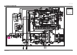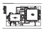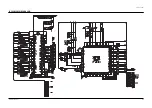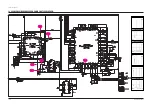
Samsung Electronics
10-9
Glossary
Phosphor degradation
:
Gradual decline in fluorescence efficiency according to operating expectancy.
Phosphor layer
:
Thin layer made up of phosphor. FluorescencPle substance must be thick enough to optimize transferring
the ultraviolet rays from plasma discharge to visible light
Pixel, picture element
:
The smallest unit that can display the entire range of luminance and chromaticity. Generally, pixel consists
of sub pixels (or dots).
Pixel arrangement
:
Expression of sub pixels within a pixel.
Pixel count
:
The number of pixels that make up a display. It is described as the number of column pixels against the
number of row pixels.
Pixel pitch
:
The distance between the centers of the two closest pixels. Move as far as the pitch and reach the identical
location.
Plasma display
:
Electrically driven display device for causing electric discharge in gas within device. Electric energy gener-
ates light with atomic light release or from proper colored fluorescence substance.
Positive column discharge
:
The plasma area for long glow discharge. This area is a low electric field but relatively electric conductive
plasma area.
Pre discharge
:
Cell’s state where pre discharge is taking place. In this case, cell’s state becomes electric conductive due to
formation of discharge generated by ionization process of gas.
Priming
:
The stage where ions are generated for forming discharge. Generally, this is required for injection.
Priming pulse
:
Electric waveform to define the proper conditions for the next cell discharge.[symbol : Pp]
Priming voltage
:
Voltage of priming pulse.[symbol : Vp]
Protecting layer
:
The layers applied to the device function constituents (for example, fluorescence, electrode and glass lay-
ers).
Quantum efficiency
:
Substrates farther from the viewers. These can be opaque.
Rear substrate
:
Efficiency measurement that is directly expressed with the number of output particles against the number
of input particles. In case of plasma panel, the number of photons in visible area, generated from photons
in ultraviolet area
Summary of Contents for PPM42S2X/XAA
Page 2: ...ELECTRONICS Samsung Electronics Co Ltd APR 2002 Printed in Korea AA82 ...
Page 10: ...3 2 Samsung Electronics MENO ...
Page 25: ...Circuit Operation Description Samsung Electronics 5 3 5 1 2 D PDP PS 42 BLOCK DIAGRAM ...
Page 38: ...Circuit Operation Description 5 16 Samsung Electronics 5 2 3 D DRIVER CIRCUIT DIAGRAM ...
Page 39: ...Circuit Operation Description Samsung Electronics 5 17 5 2 3 E DRIVER BOARD CONNECTOR LAYOUT ...
Page 40: ...Circuit Operation Description 5 18 Samsung Electronics ...
Page 41: ...Circuit Operation Description Samsung Electronics 5 19 ...
Page 42: ...Circuit Operation Description 5 20 Samsung Electronics ...
Page 43: ...Circuit Operation Description Samsung Electronics 5 21 ...
Page 44: ...Circuit Operation Description 5 22 Samsung Electronics ...
Page 45: ...Circuit Operation Description Samsung Electronics 5 23 ...
Page 46: ...Circuit Operation Description 5 24 Samsung Electronics ...
Page 47: ...Circuit Operation Description Samsung Electronics 5 25 ...
Page 48: ...Circuit Operation Description 5 26 Samsung Electronics ...
Page 49: ...Circuit Operation Description Samsung Electronics 5 27 ...
Page 50: ...Circuit Operation Description 5 28 Samsung Electronics ...
Page 51: ...Circuit Operation Description Samsung Electronics 5 29 ...
Page 52: ...Circuit Operation Description 5 30 Samsung Electronics ...
Page 82: ...Circuit Operation Description 5 60 Samsung Electronics ...
Page 83: ...Circuit Operation Description Samsung Electronics 5 61 ...
Page 84: ...Circuit Operation Description 5 62 Samsung Electronics MEMO ...
Page 93: ...Exploded View Parts List Samsung Electronics 7 1 7 Exploded View Parts List 7 1 PPM42S2X XAA ...
Page 106: ...Electrical Parts List 8 12 Samsung Electronics MEMO ...
Page 128: ...10 14 Samsung Electronics MEMO ...
Page 130: ...11 2 Samsung Electronics MENO ...
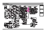
Page 133: ...Samsung Electronics Schematic Diagrams 12 3 TP01 12 3 SCALER3 3D COMB FILTER TP01 CVBS IN ...
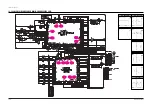
Page 134: ...Schematic Diagrams 12 4 Samsung Electronics 12 4 SCALER4 VIDEO DECODER PIP FIRST IN OUTPUT ...
Page 135: ...Samsung Electronics Schematic Diagrams 12 5 12 5 SCALER5 VIDEO DA CON ...
Page 141: ...Samsung Electronics Schematic Diagrams 12 11 12 11 SOUND ...
Page 143: ...Samsung Electronics Schematic Diagrams 12 13 12 13 CONTROL REMOCON CONTROL REMOCON ...

