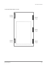
5-2-3(A) FUNCTIONS OF EACH BOARD
(1) X board
X board is connected to the panel’s X-electrode blocks, 1) generates sustain voltage pulse (including
ERC), 2) generates X rising ramp pulse, and 3) sustains Ve bias during scan period.
(2) Y board
Y board is connected to the Y-electrode blocks of panel, 1) generates sustain voltage pulse (including
ERC), 2) generates Y rising and falling ramp pulse, and 3) sustains Vscan bias.
(3) Y buffer board (upper and lower)
Y buffer board impresses scan pulse to Y electrodes, and consists of upper and lower sub-boards. In
case of SD class, one board is equipped with 4 scan driver IC’s (STMicroelectronics STV7617 with 64
or 65 outputs).
(4) COF
Impresses Va pulse on address electrodes in the address section and generates address discharge
based on a difference between such Va pulse and scan pulse impressed on Y electrodes. It is in the
form of COF, and a COF is equipped with 4 data drive IC’s (STMicroelectronics STV7610A with 96
outputs). For a single scan, 7 COF’s are required.
Circuit Operation Description
5-12
Samsung Electronics
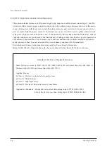
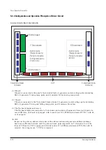
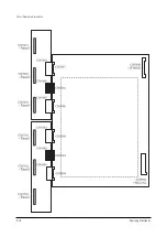
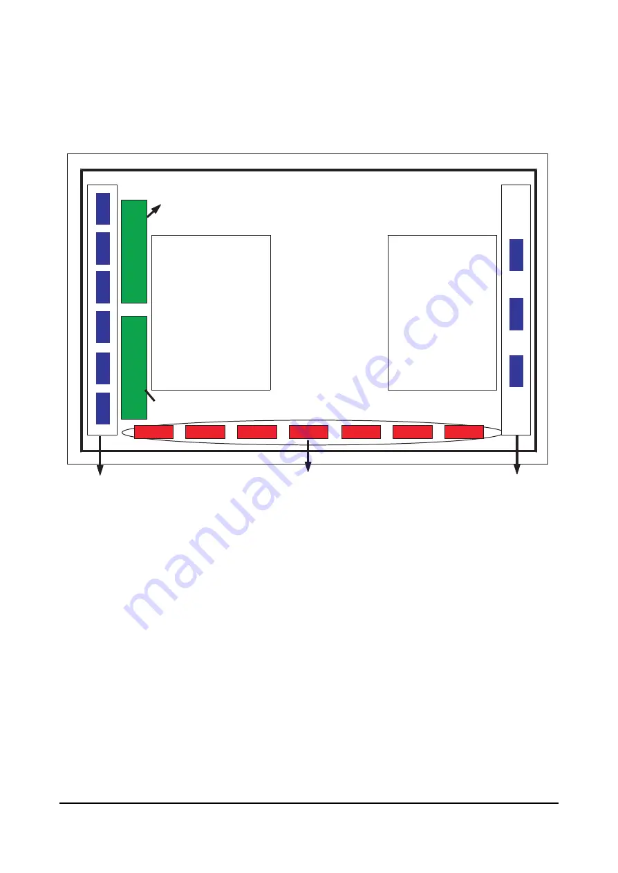
5-2-3 Configuration and Operation Principles of Driver Circuit
Y-Buffer (Upper)
Y-Buffer (Lower)
Y Drive board
- Sustain pulse
(Energy recovery)
- Rising ramp pulse
- Falling ramp pulse
- Vscan pulse
X Drive board
- Sustain pulse
(Energy recovery)
- Rising ramp pulse
- Ve bias
Y-electrode blocks
(6 blocks)
COF
X-electrode blocks
(3 blocks)
Summary of Contents for PPM42S2X/XAA
Page 2: ...ELECTRONICS Samsung Electronics Co Ltd APR 2002 Printed in Korea AA82 ...
Page 10: ...3 2 Samsung Electronics MENO ...
Page 25: ...Circuit Operation Description Samsung Electronics 5 3 5 1 2 D PDP PS 42 BLOCK DIAGRAM ...
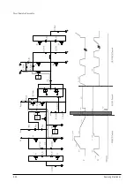
Page 38: ...Circuit Operation Description 5 16 Samsung Electronics 5 2 3 D DRIVER CIRCUIT DIAGRAM ...
Page 39: ...Circuit Operation Description Samsung Electronics 5 17 5 2 3 E DRIVER BOARD CONNECTOR LAYOUT ...
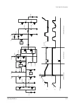
Page 40: ...Circuit Operation Description 5 18 Samsung Electronics ...
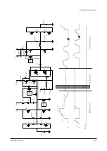
Page 41: ...Circuit Operation Description Samsung Electronics 5 19 ...
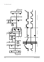
Page 42: ...Circuit Operation Description 5 20 Samsung Electronics ...
Page 43: ...Circuit Operation Description Samsung Electronics 5 21 ...
Page 44: ...Circuit Operation Description 5 22 Samsung Electronics ...
Page 45: ...Circuit Operation Description Samsung Electronics 5 23 ...
Page 46: ...Circuit Operation Description 5 24 Samsung Electronics ...
Page 47: ...Circuit Operation Description Samsung Electronics 5 25 ...
Page 48: ...Circuit Operation Description 5 26 Samsung Electronics ...
Page 49: ...Circuit Operation Description Samsung Electronics 5 27 ...
Page 50: ...Circuit Operation Description 5 28 Samsung Electronics ...
Page 51: ...Circuit Operation Description Samsung Electronics 5 29 ...
Page 52: ...Circuit Operation Description 5 30 Samsung Electronics ...
Page 82: ...Circuit Operation Description 5 60 Samsung Electronics ...
Page 83: ...Circuit Operation Description Samsung Electronics 5 61 ...
Page 84: ...Circuit Operation Description 5 62 Samsung Electronics MEMO ...
Page 93: ...Exploded View Parts List Samsung Electronics 7 1 7 Exploded View Parts List 7 1 PPM42S2X XAA ...
Page 106: ...Electrical Parts List 8 12 Samsung Electronics MEMO ...
Page 128: ...10 14 Samsung Electronics MEMO ...
Page 130: ...11 2 Samsung Electronics MENO ...
Page 133: ...Samsung Electronics Schematic Diagrams 12 3 TP01 12 3 SCALER3 3D COMB FILTER TP01 CVBS IN ...
Page 134: ...Schematic Diagrams 12 4 Samsung Electronics 12 4 SCALER4 VIDEO DECODER PIP FIRST IN OUTPUT ...
Page 135: ...Samsung Electronics Schematic Diagrams 12 5 12 5 SCALER5 VIDEO DA CON ...
Page 141: ...Samsung Electronics Schematic Diagrams 12 11 12 11 SOUND ...
Page 143: ...Samsung Electronics Schematic Diagrams 12 13 12 13 CONTROL REMOCON CONTROL REMOCON ...

