background image

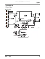
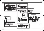
CN5401

CN5402

CN5403

CN5412

CN5501

CN5502

CN5503

CN5407

CN5507

CN5701

CN5707

CN807

CN809

CN808

CN810

CN4701

CN4002

CN4001

CN4000

CN4004

CN2004

CN2600

CN2610

CN2510

CN1

CN3

CN800

LOGIC BOARD

SMPS

X-DRIVE

Y-DRIVE

Y-MAIN SCAN(HIGH)

F-BUFFER

FUNCTION

POWER SW

Y-MAIN SCAN(LOW)

CN2609

CN2003

CN2000

CN2001

CN2006

CN2005

SPEAKER

CN801

CN2002

MAIN BOARD

CN2500

CN2509

E-BUFFER

4

5

6

7

8

10

11

9

CN1101

CN2202_HD

CN1605_PDP

CN1606 CN1203

2

1

AC-INLET

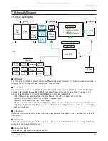
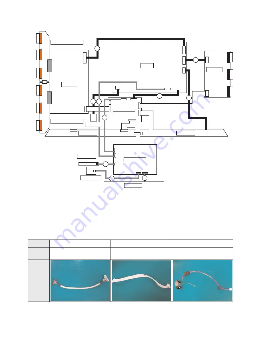
<50" Overall Wiring>

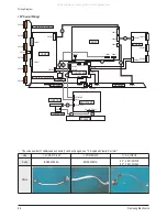
The code number of cable(Lead-connector) can be changed, see "5. Exploded View & Part List." 

Wiring Diagram

6-2

Samsung Electronics

Use

LVDS 31P-30P

POWER 24P

AC_INPUT

Code

BN39-00859A

BN39-00881A

42" - 2901-001378
50" - 2901-001340

Photo

All manuals and user guides at all-guides.com

Summary of Contents for PS50C62HX

Page 1: ...oting 5 Exploded View Part List 6 Wiring Diagram 7 Schematic Diagram SERVICE Manual PS 50C62HX PDP TELEVISION Chassis F33B P_Europe_HD _Lily2 Ready Model PS50C62HX XEC Refer to the service manual in t...

Page 2: ...nics Co Ltd Oct 2007 Printed in Korea AA82 04876A Area Web Site North America service samsungportal com Latin America latin samsungportal com CIS cis samsungportal com Europe europe samsungportal com...

Page 3: ...2 3 Accessories 2 3 Chapter 3 Disassembly Reassembly 3 1 Overall Disassembly Reassembly 3 1 Chapter 4 Troubleshooting 4 1 Troubleshooting 4 1 4 2 Adjustment 4 16 4 3 Upgrade 4 31 Chapter 5 Exploded V...

Page 4: ...the product can only be repaired safely when the chassis is connected to the earth end of the AC power source To make sure the AC power cord is properly connected follow the instructions below Use the...

Page 5: ...egular one the safety or protective features will be lost even if the new one has a higher voltage or more watts Critical safety parts should be bracketed with Use only regular parts for replacements...

Page 6: ...e of the AC plug and that of the conductive material should be more than 1 7 Any B interlock should not be damaged If the metal heat sink is not properly installed no connection to the AC power should...

Page 7: ...s 6 Use only anti static solder removal devices Most solder removal devices do not support an anti static feature A solder removal device without an anti static feature can store enough static electri...

Page 8: ...lso check the antenna cable or the external connectors if they are fully unplugged Damage to the cord may cause fire or electric shock 6 Keep the antenna far away from any high voltage cables and inst...

Page 9: ...1 6 Samsung Electronics MEMO All manuals and user guides at all guides com...

Page 10: ...62H PS 50C62H Screen Size 42 Inches 16 9 50 Inches 16 9 Dimensions WxHxD 1155 x 440 x 878 mm With Stand 1355 x 460 x 984 mm With Stand Weight 42 8 kg With Stand 53 9 kg With Stand Voltage AC 100 240V...

Page 11: ...trast Ratio 10000 1 10000 1 10000 1 10000 1 Image Enhacer FBE2X FBE2X FBE2X FBE2X Audio Equalizer O O O O Auto Volume O O O O Surround Sound SRS TruSurround SRS TruSurround SRS TruSurround SRS TruSurr...

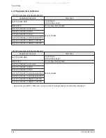
Page 12: ...ard Safety Guide Manual BN68 00514E AA68 03575D AA68 03242K Ferrite Core for Earphone Power Cord 3301 001110 Ferrite Core for S VIDEO Power Cord 3301 001305 Accessories that can be purchased additiona...

Page 13: ...2 4 Samsung Electronics MEMO All manuals and user guides at all guides com...
Page 14: ...capacitors first when separating PCB s with high capacity capacitors such as SMPS X Main Board Y Main Board etc A spark may be generated by the electric charge and there is danger of electronic shock...

Page 15: ...R EMI AC LINE Detach connector from Main SMPS Remove 2 screws PH WWP M3 L8 NI PLT Remove a screw BH S M4 L10 ZPC BLK Remove FILTER EMI AC LINE 3 1 4 Separation of BRACKET PCB Part Name Description Des...

Page 16: ...BLK Remove 6 screws BH S M4 L10 ZPC BLK Remove Wall Bracket Please lay the PDP panel face down on a soft surface when separating front cover 50 Wall Bracket Remove 2 screws BH B M4 L3 ZPC BLK Remove 6...

Page 17: ...4 0 L3 ZPC BLK SWRCH18A Remove the Speaker 50 Speaker Remove 4 screws BH WP B M4 0 L3 ZPC BLK SWRCH18A Remove the Speaker 3 1 7 Separation of ASSY BOARD P POWER IR Part Name Description Description Ph...

Page 18: ...the power board as there may be some remaining electrical charge in the capacitor Specifically avoid touching any part of the capacitor 50 SMPS Detach all connectors from the SMPS Remove 8 screws PH...

Page 19: ...on Description Photo 42 Logic Board Detach all connectors from the Logic Main Board Remove 4 screws WSP PH M3 L8 NI PLT Remove the Logic Main Board 50 Logic Board Detach all connectors from the Logic...

Page 20: ...Cable Detach all Connectors from the X Main Board To separate the Flat Cable of the X Board press the upper and the lower sides of the connector 42 X Main Board Remove 4 screws PH WWP M3 L8 NI PLT Re...

Page 21: ...Name Description Description Photo Flat Cable Detach the 6 scan board connectors from the panel by pulling the holder from both the top and bottom ends 42 Y Scan Board Remove 3 screws PH WWP M3 L8 NI...

Page 22: ...iption Description Photo 42 Y Main Board Remove 4 screws PH WWP M3 L8 NI PLT Detach all connectors from the Y Main Board 50 Y Main Board Remove 4 screws PH WWP M3 L8 NI PLT Detach all connectors from...

Page 23: ...emove the Still Bar 50 Still Bar Remove 4 screws PH WWP M3 L8 NI PLT Remove the Still Bar 42 Buffer Board Detach the all connectors from the buffer board Remove 3 screws PH WWP M3 L8 NI PLT Remove the...

Page 24: ...oto Function Board Remove 2 screws BH B M4 L3 ZPC BLK Remove the Function Board 3 1 13 Separation of ASSY PANEL BRACKETS Part Name Description Description Photo Panel Brackets Remove 3 screws BH B M4...

Page 25: ...3 12 Samsung Electronics MEMO All manuals and user guides at all guides com...
Page 26: ...to see if there is a disconnected or loose cable connection Check to see if the cables are connected according to the connection diagram 2 Check the power input to the Main Board 3 Check the voltage i...

Page 27: ...connected or the Main Board or SMPS is not functioning In this case check the following Check the internal cable connection Check the fuses Check the output voltage of the SMPS Replace the Main Board...

Page 28: ...y connecting the cables one by one Troubleshooting Procedures Caution When separating and connecting the cables such as CN810 CN809 CN808 CN807 of the Main SMPS CN4701 of the X Main Board and CN5707 o...

Page 29: ...the cables such as CN810 CN809 CN808 CN807 of the Main SMPS CN4701 of the X Main Board and CN5707 of the Y Main Board a spark may be generated by the electric charge of the high capacity capacitor Th...

Page 30: ...unctioning Speaker defect Troubleshooting Procedures Is the cable connection between the Main Board and the speaker properly connected Connect the cable properly or replace the cable if necessary Is t...

Page 31: ...Checklist Check the antenna connection settings Check the CVBS cable connection Check the power input of the Main board Troubleshooting Procedures Is the antenna connection setting properly configured...

Page 32: ...er ON VA Multi Abnormal Abnormal Normal VS ON VS Normal Abnormal Check the Other board Image Board or Driver Board or Cable Check the SUB2 QX801 QX802 Check the SUB1 QS801 QS802 Check the 5 3V ICX808...

Page 33: ...t is no screen Y MAIN X MAIN Logic Main Sustain Open Some horizontal lines don t exist on screen Scan Buffer FPC of X Y Sustain Short Some horizontal lines appear to be linked on screen Scan Buffer FP...

Page 34: ...Check the FUSE Check the input voltage YES NO YES NO Y MAIN Check several points FUSE FET DIODE Y MAIN Normal State Replace the Board Replace the Board OK OPEN SHORT OK F5001 for VDD F5002 for Vs F500...

Page 35: ...K OPEN SHORT OK F5001 for VDD F5002 for Vs F5004 for VCC F5005 for OUT_L Q5009 Q5021 X MAIN Check several points FUSE FET X MAIN Normal State Replace the Board Replace the Board OK OPEN SHORT OK F4001...

Page 36: ...efect is from Y buffer Replace the Panel There is a defect on the FPC OK NG Sustain Short some horizontal lines appear to be linked on Video Y FPC Sustain Short Discharging in unwanted Scan line After...

Page 37: ...ormal Reload the data onto the MICOM and recheck it Check if there is an open or short circuit on the Buffer Board and the Logic Main address data output section Check the FFC connection status Check...

Page 38: ...ers E F COF defect burnt Replace the module A green screen appears when the TV is turned on The Scale is not reseting Replace the Main board The OSD box appears but there is no text Incorrect program...

Page 39: ...eplace the Main board A vertical green line appears on the screen The SMPS voltage is incorrect Adjust the SMPS voltage according to the voltage printed on the module label Dim screen blurred in red X...

Page 40: ...MODULE P Y MAIN SCAN BUFFER Row Bar screen is blank 6 ASSY PDP MODULE P ADDRESS E BUFFER Corresponding Buffer Board block screen is blank 7 ASSY PDP MODULE P ADDRESS F BUFFER Corresponding Buffer Boa...

Page 41: ...djustment equipment is available PDP Option of Factory Mode set the Factory Data Type item as the suitable value of relevant model Adjust Calibration of Factory Mode for each mode Adjust White Balance...

Page 42: ...higher level mode Using the Numeric 0 9 keys you can select a channel Using the SOURCE key you can switch AV modes 5 Initial SERVICE MODE DISPLAY State The version of the firmware displayed at the bot...

Page 43: ...Call Lily Brod Plus Jasmine Anynet OFF ON OFF Auto Power ON ON OFF Nordic ON ON OFF LNA Menu OFF ON OFF TTX On Off ON ON OFF TTX List FLOF FLOF List Carrier Mute OFF ON OFF High Devi OFF ON OFF Volume...

Page 44: ...t 00H FFH 128 128 128 128 R Gain 00H FFH 128 128 128 128 G Gain 00H FFH 128 128 128 128 B Gain 00H FFH 128 128 128 128 4 MST68981 ADC Calibration Item Range Tv AV Scart CVBS Y Gain 128 0 255 CVBS Y Of...

Page 45: ...Target Low 17 0 255 High 234 0 255 Delta 3 0 255 Pc ADC Target Low 1 0 255 High 254 0 255 Delta 3 0 255 All ADC Target Low 2 0 255 High 235 0 255 Delta 1 0 255 Item Range Tv AV Scart H1 Gain 28 H2 Gai...

Page 46: ...128 128 128 128 ACR Offset 0 128 15 15 15 15 15 15 15 15 ACR Th1 0 255 30 30 30 30 30 30 30 30 ARC Th2 0 255 130 130 100 130 130 130 130 130 Skin Enable 0 1 1 1 1 1 1 1 1 1 Skin Tu 0 255 165 165 150...

Page 47: ...Check 1 1 60 Num of Double Check 5 5 60 Mono Weight 1 1 20 Stereo Weight 1 1 20 Dual Weight 1 1 20 BG M2S Threshold 144 0 255 DK M2S Threshold 80 0 255 BG S2M Threshold 176 0 255 DK S2M Threshold 0 0...

Page 48: ...N IDTV LVDS ON FBE Select FBE2X FBE2X FBE Tuner ALPS ALPS SEMCO AUTO Tuner TOP Semco 10 1 30 Tuner TOP Alps 13 D Gamma 22 M Gamma OFF OFF 0 88 0 95 A Watchdog OFF ON OFF Hp Detect LOW LOW HIGH PDP FRC...

Page 49: ...55 142 143 149 142 142 W2_BGAIN 0 255 48 47 93 51 48 W2_R_OFFS 0 255 129 127 124 128 129 W2_B_OFFS 0 255 143 145 110 143 143 NO_RGAIN 0 255 141 139 137 141 141 NO_BGAIN 0 255 104 102 123 104 104 NO_R_...

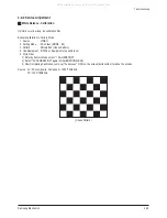
Page 50: ...3 Pattern Pattern 24 Chess Pattern 4 Use Equipment K 7256 or Equipment of equality level 5 Work order 1 Enter by Factory Mode select 1 CALIBRATION 2 Select AV CALIBRATION again in CALIBRATION MENU 3 A...

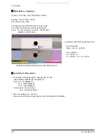
Page 51: ...n MSPG 945 Series Pattern 16 Color temperature 1500K 500 6 20 MPCD Color coordinate H L 270 280 2 L L 270 280 3 2 1 Ft 0 05 Ft SAMSUNG WHITE BALANCE Adjustment PATTERN with FPD Conditions for Measurem...

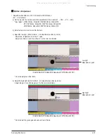
Page 52: ...a c Adjust the low light Refer to table 1 2 in adjustment position by mode Adjust sub Brightness to set the Y value Adjust red offset x and blue offset y to the color coordinates Do not adjust green o...

Page 53: ...ing each Replaced assembly items Check Items ASSY PCB MISC MAIN 1 Auto Program 2 White Balance Adjust SMPS PDP TV Vs Va voltage check and adjust ASSY PDP MODULE P LOGIC MAIN Not to be adjusted ASSY PD...

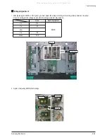
Page 54: ...int Vs Test point Value Board Adjustment Vs 210 SMPS Va 63 Vset Ve 94 Vscan 190 Voltage Adjustment 1 After replacing the SMPS or PDP panel you must adjust the voltage referring to the voltage label pr...

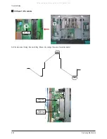
Page 55: ...RR and Y FR controls 60usec 80usec Test Point Rising ramp variable resistor Falling ramp variable resistor Set the main reset rising 60usec falling 80usec by change the value of variable resistor All...

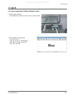
Page 56: ...232C Cable 1 Installthe Flash Downloader ConnectSet Service Jack and Jig Cable to execute Program Update 2 Flash Downloader program update Turn on the TV Set Click Connect icon on the MSTAR tool Click...

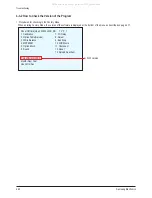
Page 57: ...ware is displayed at the bottom of the menu as described on page 4 17 Panel ON time Hour 00002 L24E_RS TV P 1 1 Calibration 7 YC Delay 2 Option Table Service 8 Adjust 3 White Balance 9 Bus Stop 4 MST6...

Page 58: ...MEMO Samsung Electronics 4 33 All manuals and user guides at all guides com...
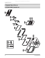
Page 59: ...Part List 5 Exploded View Part List 5 1 PS50C62HX XEC Exploded View M0112 T0023 T0061 T0023 T0059 T0603 CIS7 M0145 T0456 T0044 M0107 T0079 M0111 M0115 M0027 T0074 T0268 M0150 T0003 T0175 M0013 All man...

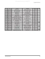
Page 60: ...SY BRACKET P FILTER BOTTOM 50C7 AL 1 S A T0003 BN96 03124G ASSY COVER P FRONT 50C62HX XEC HIPS HB 1 S A T0023 BN96 03173A ASSY COVER P KNOB POWER 42P7 ABS 1 S A T0023 BN64 00459A KNOB POWER 42P7 PC Vi...

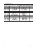
Page 61: ...GIC MAIN BOARD S50HW YB02 L 1 T0044 BN96 06516A ASSY PDP MODULE P S50HW YB02 PL50HW026A 1 T0045 BN96 06518A ASSY PDP P X MAIN BOARD S50HW YB02 X Mai 1 T0047 BN96 06520A ASSY PDP P Y MAIN SCAN UPPER S5...

Page 62: ...810 CN4701 CN4002 CN4001 CN4004 CN2004 CN2600 CN2610 CN2510 CN1 CN3 CN800 LOGIC BOARD SMPS X DRIVE Y DRIVE Y MAIN SCAN AC INLET F BUFFER FUNCTION POWER SW CN2609 CN2000 CN2001 CN2006 SPEAKER CN801 CN2...

Page 63: ...N LOW CN2609 CN2003 CN2000 CN2001 CN2006 CN2005 SPEAKER CN801 CN2002 MAIN BOARD CN2500 CN2509 E BUFFER 4 5 6 7 8 10 11 9 CN1101 CN2202_HD CN1605_PDP CN1606 CN1203 2 1 AC INLET 50 Overall Wiring The co...

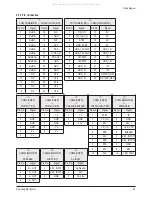
Page 64: ...22 12V 11 GND_5V 23 N C FAN_ON 12 GND_5V 24 N C FAN_DET 6 1 1 Pin Connection CN810 SMPS CN5707 Y B D Pin No Signal 1 Vg 2 GND 3 GND 4 GND 5 Vs 6 Vs CN809 SMPS CN4701 X B D Pin No Signal 1 Vg 2 GND 3 G...

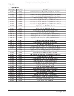
Page 65: ...age signal LVDS connect 41pin from Main Board CN800 CN800 AC Power input connect from AC inlet CN4002 CN4002 Horizontal X scan line of Module and X scan Connect first Block CN4001 CN4001 Horizontal X...

Page 66: ...oded by the Video Board outputs the ADDRESS data signal for each pattern and generates X and Y drive signals The Address Buffer Board buffers and transfers the ADDRESS data output signal using TCP IC...

Page 67: ...7 2 Samsung Electronics MEMO All manuals and user guides at all guides com...
Page 68: ...V 6 1 F n 0 0 1 1 m h o K 7 4 D C L _ 9 0 1 1 R 7 3 1 1 C 4 1 1 P T D V 3 3 B 1 _ V 5 A A C C V _ V 5 B P M A _ D N U O S F u 2 2 V 6 1 2 2 1 1 C F n 0 0 1 9 2 1 1 C D V 5 2 1 B 7 6 1 1 C F m 1 V 0 1...

Page 69: ...C 0 1 2 1 D F p 0 0 1 9 0 3 1 C 8 4 1 4 L L M P 3 0 3 1 C 100Kohm R1315 1 10W 1 10W R1313 100Kohm F n 0 0 1 m h o K 1 5 6 2 1 R 100Kohm R1311 1 10W 1 10W R1309 100Kohm 5 8 2 1 C F n 2 2 F n 1 1 10W R...

Page 70: ...h o 0 0 1 5 5 4 1 R 3 0 4 1 A J 1 2 3 1 1 9 P T 1 4 0 4 1 D E S 8 4 1 4 D B M M P O _ 1 0 5 1 D B 2 6 Z L R R1441 12Kohm m h o 0 P O _ 0 8 4 1 R P O _ 5 3 4 1 D 1 2 3 m h o 0 0 1 9 8 4 1 R 100pF C1409...

Page 71: ...1 2 0 2 U E _ 8 0 6 1 A J 1 0 1 1 1 1 10nF C1652 7 4 6 1 D 1 2 3 1 1 330pF C1613_LCD 1 D A P _ 6 4 6 1 D 1 2 3 D1615 A C C V _ V 5 B D C L _ 3 0 6 1 L F n 0 0 1 5 3 6 1 C 1 m h o 2 2 P M A L _ 0 0 7...

Page 72: ...R m h o 0 P O _ 3 4 0 2 R m h o 2 2 F I S _ V 3 3 A 8 V 3 3 A RA2027 100ohm 1 2 3 4 5 6 7 8 0 0 2 R m h o 0 U A _ V 3 3 A 0 3 8 1 C m h o 0 3 1 1 2 R 7 1 0 2 C F n 0 0 1 F n 0 0 1 100ohm R2040 F n 7...

Page 73: ...R _ 3 R _ R W P 7 D G N I R _ R _ D N G 8 D G N I R _ R _ D N G 9 D G N I R _ 1 R _ R W P 3 1 E 6 _ A 3 3 S S V A 4 1 E 3 E 1 _ A 3 3 S S V A G N I R _ 1 R _ R W P 4 E 0 1 D G N I R _ R _ D N G 1 1 D...

Page 74: ...7 C F p 0 2 2 4 0 0 3 R m h o K 0 1 H u 5 1 2 0 0 7 L V T D _ V 3 3 B 7 0 0 3 R m h o K 2 1 T E S E R T E S E R 1 D N G 2 D D V 3 V P 2 4 C 8 1 8 9 T R 3 0 0 3 C I V T D _ V 3 3 B F E R X F u 1 1 1 0...

Page 75: ...1 1 m h o 0 0 1 1 1 1 3 R F n 0 0 1 4 0 1 3 C V 6 1 m h o 0 1 9 9 0 1 3 R W 0 1 1 0 1 1 3 R m h o 0 1 9 W 0 1 1 W 0 1 1 m h o 5 7 6 2 1 3 R W 0 1 1 6 1 1 3 R m h o 5 7 W 0 1 1 4 2 1 3 R m h o 5 7 1 6...

Page 76: ...B D C L _ 2 0 2 3 L H u 0 1 0 1 2 3 D B T J 1 2 1 8 0 6 1 M 1 B H B m h o K 0 1 1 0 2 3 R 6 2 2 3 R m h o K 0 1 F n 0 0 1 5 4 2 3 C F n 0 0 1 6 0 2 3 C V 6 1 5 0 2 3 C F n 0 0 1 V 6 1 V 6 1 F n 0 0 1...

Reviews: