I/O PORTS
S3C80A5B
9-2
PORT DATA REGISTERS
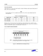
Table 9-2 gives you an overvi ew of the register locations of all three S3C80A5B port data registers. Data registers for
ports 0, and 1 have the general format.
NOTE
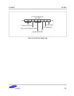
The data register for port 2, P2, contains three bits for P2.0, P2.1 and P2.2, and an additional status bit for
carrier signal on/off.
Table 9-2. Port Data Register Summary
Register Name
Mnemonic
Decimal
Hex
R/W
Port 0 data register
P0
224
E0H
R/W
Port 1 data register
P1
225
E1H
R/W
Port 2 data register
P2
226
E2H
R/W
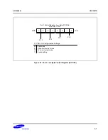
Because port 2 is a 3-bit I/O port, the port 2 data register only contains values for P2.0, P2.1 and P2.2. The P2
register also contains values for P2.0, P2.1 and P2.2. The P2 register also contains a special carrier on/off bit(P2.5).
See the port 2 description for details. All other S3C80A5B I/O ports are 8-bit.
PULL-UP RESISTOR ENABLE REGISTERS
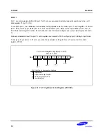
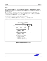
Pull-up Resistor Enable Register (PnPUR, where n = 0, 1)
(E7H, ECH), R/W
.7
.6
.5
.4
.3
.2
.1
.0
MSB
LSB
NOTE:
Pull-up resistors can be assigned to the port 2 pins, P2.0, P2.1 and P2.2
by marking the appropriate the port 2 control register, P2CON.
Pn.7
Pn.6
Pn.5
Pn.4
Pn.3
Pn.2
Pn.1
Pn.0
Pull-up resistor enable bit:
0 = Disable pull-up resistor
1 = Enable pull-up resistor
Figure 9-1. S3C80A5B I/O Port Data Register Format


