SAMSUNG Proprietary-Contents may change without notice
2-2
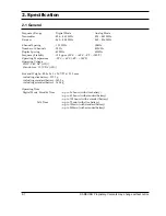
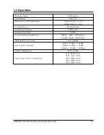
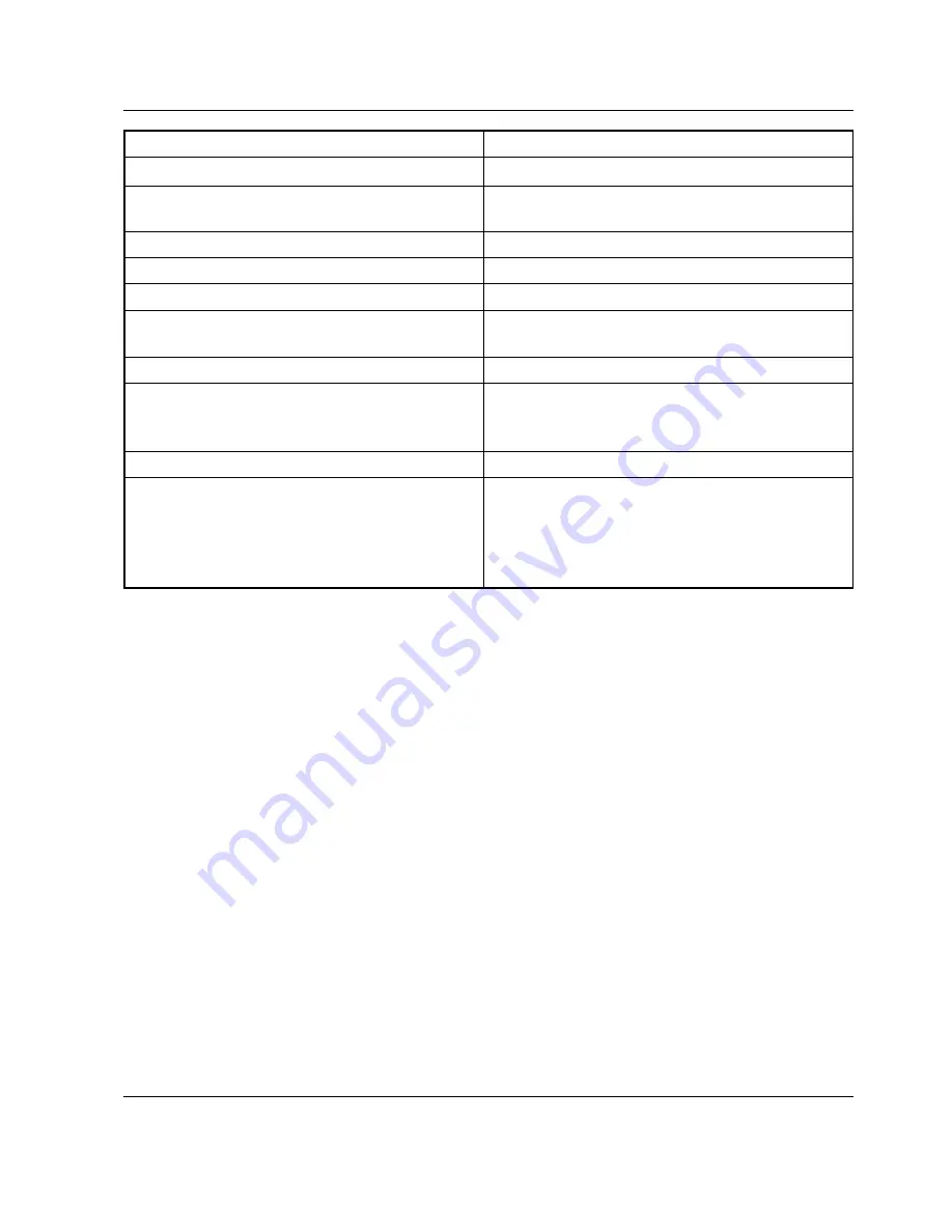
2-2 Digital Mode
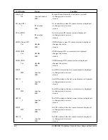
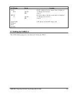
Waveform Quality
0.944 or more
Time Reference
±1uS or less
Rx Sensitivity and Dynamic Range
-104dBm, FER=0.5% or less
-25dBm, FER=0.5% or less
Tx Output Power
320mW (25dBm)
Tx Frequency Deviation
±300Hz or less
Occupied Band Width
1.32MHz
Tx Conducted Spurious Emission
900KHz : -42dBc / 30KHz below
1.98MHz: -54dBc / 30KHz below
Minimum Tx Power Control
below -50dBm
-25dBm: -57.0dBm ~ -38.5dBm
Open Loop Power Control
-65dBm: -17.5dBm ~ + 1.5dBm
-104dBm: +18.0dBm ~ +30.0dBm
Standby Output Power
below -61dBm
Test1: ±24dB or less
Test2: 0mS ~ 2.5mS
Colsed Loop Tx Power Control Range
Test3: ±24dB or more
Test4: ±24dB or more
Test5: ±24dB or more
Summary of Contents for SCH-811
Page 2: ...Samsung Electronics Co Ltd GH68 00398A 1999 3 REV 1 0 ELECTRONICS ...
Page 84: ...9 1 Cellular Phone 9 1 1 Main PCB LOGIC B D 9 PCB Diagrams ...
Page 85: ...9 1 Cellular Phone 9 1 2 Main PCB LOGIC B D ...
Page 86: ...9 1 Cellular Phone 9 1 3 Main PCB RF B D ...
Page 87: ...9 1 4 LCD FPC ...
Page 88: ...9 2 Desk Top rapid Charger PCB Top View ...
Page 89: ...Bottom View ...
Page 90: ...9 3 Hands Free kit 1 PCB Top View ...
Page 91: ...Bottom View ...
Page 92: ...9 4 Cradle 1 PCB Top View ...
Page 93: ...9 5 TC PCB Top View Bottom View ...
Page 94: ...9 6 CLC PCB Top View Bottom View ...
Page 98: ...10 4 Travel Charger Block Diagram ...
Page 102: ...10 5 Main Circuit Diagram 1 3 ...
Page 103: ...Main Circuit Diagram 2 3 ...
Page 104: ...Main Circuit Diagram 3 3 ...
Page 105: ...LCD FPC Circuit Diagram ...
Page 106: ...10 7 Hands Free kit 1 Circuit Diagram data ...
Page 107: ...Hands Free kit 1 Circuit Diagram audio ...
Page 108: ...Car Adaptor 1 Circuit Diagram ...
Page 109: ...10 8 Cradle 1 Circuit Diagram ...
Page 110: ...10 9 Travel Charger Circuit Diagram ...
Page 111: ...10 10 CLC Cigarette Lighter Charger Circuit Diagram ...

