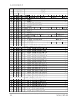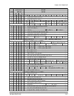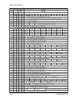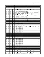
Samsung Electronics
4-22
Alignment and Adjustment
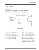
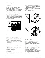
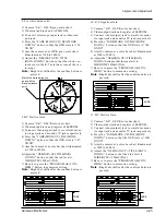
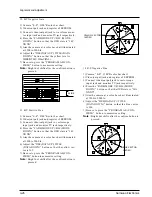
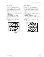
1. Focus to zoom tracking
Notes :
To maintain proper focus throughout the zoom range, the focus lens position must be changed as
the zoom lens is moved.
During this adjustment the microprocessor will measure the focus positioning requirements at the
wide and telephoto position of the zoom lens.
1) Camera “E-E”.
2) Focus chart (Attached on the last page of this manual).
3) Aim the camera at the focus chart placed 3 meters away and perpendicular to the center of the lens.
The chart should be placed on the flat, gray or white wall.
4) Connect monitor TV jack to video output jack.
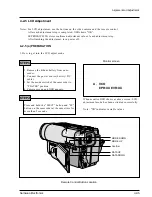
5) Press the “FADE(MODE UP)” and “BLC(MODE DOWN)” button, so that the OSD start is “0DE. 3M
LENS XX XX”.
6) Press “PROGRAM AE(CONFIRM)” button.
The camera will move both zoom and focus lens.
The adjustment is finished when the O.K! message appears on the TV screen.
Store the data to mode 0A6, 0A7, 0A8, 0A9, 0AA, 0AB, 0AC or 0AD.
4-2-2 Camera System Adjustment
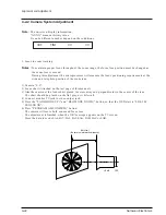
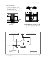
(3M
±
1cm)
(Be sure to maintain the distance.)
LENS
CCD
Note :
The on-screen display information.
“XX XX” means arbitrary value.
It can be different number depend on the conditions.
0DF T.INI XX XX
Summary of Contents for SCL500
Page 1: ...SERVICE MANUAL SAMSUNG VPL500 MODEL ...
Page 7: ...MEMO MEMO Products Specifications and Comparison Chart Samsung Electronics 2 4 ...
Page 85: ...Samsung Electronics 5 18 Exploded View and Parts List MEMO MEMO ...
Page 115: ...7 2 Samsung Electronics PCB Diagrams 7 1 Main PCB Normal Component Side ...
Page 116: ...7 3 Samsung Electronics PCB Diagrams ...
Page 117: ...7 4 Samsung Electronics PCB Diagrams 7 2 Main PCB Normal Conductor Side ...
Page 118: ...7 5 Samsung Electronics PCB Diagrams ...
Page 119: ...7 6 Samsung Electronics PCB Diagrams 7 3 Main PCB Hi8 Component Side ...
Page 120: ...7 7 Samsung Electronics PCB Diagrams ...
Page 121: ...7 8 Samsung Electronics PCB Diagrams 7 4 Main PCB Hi8 Conductor Side ...
Page 122: ...7 9 Samsung Electronics PCB Diagrams ...
Page 124: ...7 11 Samsung Electronics PCB Diagrams 7 6 CCD PCB Component Side Conductor Side ...
Page 125: ...7 12 Samsung Electronics PCB Diagrams 7 7 CVF PCB Component Side Conductor Side ...
Page 126: ...7 13 Samsung Electronics PCB Diagrams 7 8 EVF PCB Component Side Conductor Side ...
Page 127: ...7 14 Samsung Electronics PCB Diagrams 7 9 Function PCB Component Side Conductor Side ...
Page 128: ...7 15 Samsung Electronics PCB Diagrams 7 10 LCD PCB Component Side Conductor Side ...
Page 129: ...7 16 Samsung Electronics PCB Diagrams 7 11 Front PCB ...
Page 130: ...8 1 Samsung Electronics 8 Wiring Diagram ...
Page 131: ...8 2 Samsung Electronics Wiring Diagram MEMO MEMO ...
Page 135: ...9 4 Samsung Electronics Schematic Diagrams 9 1 DC DC Converter Main ...
Page 136: ...9 5 Samsung Electronics Schematic Diagrams 9 2 System Control Servo Main ...
Page 137: ...9 6 Samsung Electronics Schematic Diagrams 9 3 Video Normal Main ...
Page 138: ...9 7 Samsung Electronics Schematic Diagrams 9 4 Video Hi8 Main ...
Page 139: ...9 8 Samsung Electronics Schematic Diagrams 9 5 Audio Main ...
Page 140: ...9 9 Samsung Electronics Schematic Diagrams 9 6 Camera Main ...
Page 141: ...9 10 Samsung Electronics Schematic Diagrams 9 7 Rear ...
Page 142: ...9 11 Samsung Electronics Schematic Diagrams 9 8 CCD ...
Page 143: ...9 12 Samsung Electronics Schematic Diagrams 9 9 CVF ...
Page 144: ...9 13 Samsung Electronics Schematic Diagrams 9 10 Front ...
Page 145: ...9 14 Samsung Electronics Schematic Diagrams 9 11 Function ...
Page 146: ...9 15 Samsung Electronics Schematic Diagrams 9 12 EVF ...
Page 147: ...9 16 Samsung Electronics Schematic Diagrams 9 13 LCD ...

