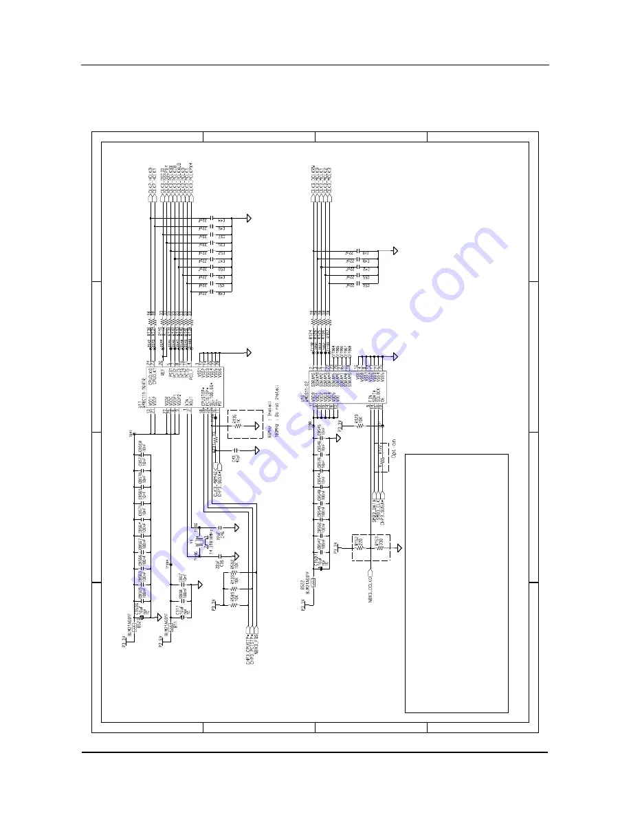
5 Schematic Diagrams and PCB Silkscreen
S820/S850
5-2
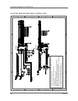
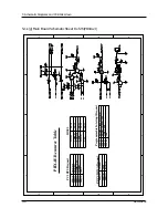
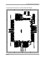
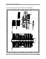
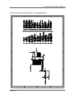
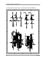
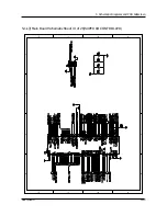
5-1-1(a) Main Board Schematic Sheet 2 of 26(Clock Chip)
4) Make trace of power pin and ground pin short and wider than width of chip pad.
7) No other signal trace across through the clock generator area.
2) Every power pins have a decoupling CAP direct connect it.
DNI
3) Ground pin directly connect to ground plane.
1) Don't place Clock chip near PCB edge. Place near PCB center and mounting hole.
Including crystal, clock chip, decoupling capacitor, damping and filter.
Make the clock generator area more "clean"
6) Clock trace must have damping resistor and filter Capacitor near to clock chip output pin.
5) Don't place via between clock chip power pin and decoupling CAP.
CK100-M
Make the shortest trace.
CKBUF-M
D
C
B
A
D
C
B
A
1
2
3
4
1
2
3
4


