
CIRCUIT DESCRIPTION
<3> EXTERNAL DMA part
This system does not use External DMA part.
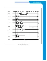
<4> DRAM control part
Since S3C46Q0X has the DRAM CONTROLLER build-in,
it may be used by connecting DRAM with external memo-
ry. The Control mode of DRAM CONTROLLER provided
by S3C46Q0X is available for EARLY WRITE, NORMAL
READ, PAGE MODE, and BYTE_HALF WORD ACCESS,
and is supported even by EDO DRAM,and SDRAM as well
as, Fast page DRAM. This system uses SDRAM, and the
signal used for READ_WRITE uses _RD,_WR signal used
for SYSTEM BUS CONTROL. It is supported with auto
REFRESH and also by the Self-refresh mode for DRAM
BACK UP. It consists of 2 Banks connected to common
_SCSO, _SCAS, _SRAS, _SCLK, _SCKE, _DQM[1:0],
each of them may use up to 2M ~ 32M HALF WORD.
In this system, Basic 2MB (TAD 8MB) is applied as system
memory. The area of DRAM is specified in the DRAM
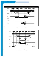
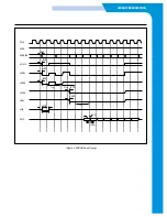
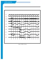
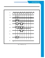
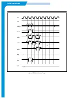
MEMORY MAP of Fig. 1, while the related TIMING DIA-
GRAM in Fig. 5, 6, 7, 8, 9.
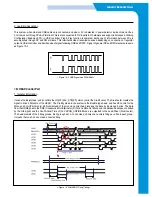
<5> RTC (REAL TIME CLOCK) part
S3C46Q0X real time clock (RTC) operates by the super
capacitor although the system power turns off. In case of
the Basic, the backup is operated with the primary battery
(CR2032), and in case of the TAD, the backup is operated
with the secondary battery (Super-cap). The RTC has the
time data that is stored as the 8 bit BCD (binary coded dec-
imal) format. The data include second, minute, hour, date,
day, month, and year. The RTC unit works with an external
32.768 kHz crystal and also can perform the alarm function
and round reset function.
<6> PARALLEL PORT INTERFACE division
This system does not use Parallel Port Interface Division.
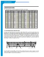
<7> USB INTERFACE PART
1. USB function description
As the mode of implementing low cost express PC
Interface, USB was applied. At USB, PC plays the role of
route hub simultaneously by existing in the highest level as
the host. That is, the device supporting each USB is con-
nected centering on PC.
The device is available for Interface for the maximum of
127. USB cable is composed of total of a set of twisted pair
and 2 power lines. The part for implementing USB function
is included in S3C46Q0X.
For Interface of USB, pull-up of 15K
Ω
is interfaced to the
data line of high level instruments, and, among data lines
of lower level instruments, pull-up resistance of 1.5K
Ω
is
interfaced to any one.
At this time, DP line is pulled up for Full Speed device, and,
for Low Speed device, DMline is pulled up. For upper level
instruments(Host, HUB) speed of device is classified inter-
faced to low level by detecting any one among DP and DM.
If both lines are in the level of GND at the same time,
device is judged that low device is not interfaced. In the
transmission mode of USB, there are (1) Control transmis-
sion, (2) Interrupt transmission, (3) Bulk transmission,
isochronous transmission. Control transmission is for Host
to find out configuration information from USB device. This
is conducted when device is interfaced. Interrupt transmis-
sion is used when small quantity of data is sent periodical-
ly. Interval value may be known from device in the case of
initial setting. Bulk transmission is valid in case of trying to
transmit data in large quantities or in case of transmitting
them accurately.
Isochronous transmission should be assured of bandwidth,
and is used when transmitting large quantities of informa-
tion. Data in voice is used where delay is not allowed but
small error is allowed. At USB coding mode and bit supping
are being conducted. First, in case original data is 1, bit
shall not change, and only when original data is 001, it shall
be inverted. Only while data is 1, 1 and 0 shall be repeat-
ed. Also, in case 1, original data, is continued in 6 bit, 0
shall be inserted, Also, in the 1st phase of packet, data in
the synchronized pattern shall be sent. About more
detailed information regarding USB,
see http//:www.usb.org.
Summary of Contents for SF-335T
Page 2: ......
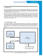
Page 19: ...CIRCUIT DESCRIPTION 2 Chorus 2 Assigned GPO Ports for RHINE ...
Page 21: ...CIRCUIT DESCRIPTION 5 HP IMPORTANT ASIC Ports for RHINE ...
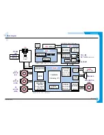
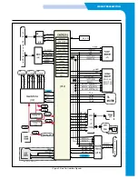
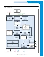
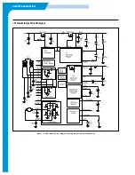
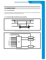
Page 24: ...CIRCUIT DESCRIPTION 3 1 5 3 Block Diagram Figure 16 Block Diagram of IP_TOP ...
Page 35: ...CIRCUIT DESCRIPTION 3 1 8 6 FM214 MODEM BLOCK DIAGRAM 3 1 8 7 FM214 VS MODEM BLOCK DIAGRAM ...
Page 36: ...CIRCUIT DESCRIPTION 3 1 8 8 FM214 SERIES MODEM PIN DESCRIPTION ...
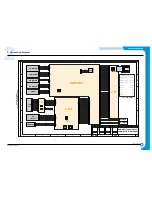
Page 48: ...4 5 Samsung Electronics SCHEMATIC DIAGRAMS Repair Manual 4 2 LIU Circuit Diagram 2002 06 25 ...