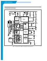
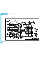
CIRCUIT DESCRIPTION
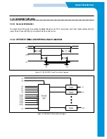
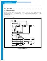
3.2.3 I/O PORT configuration and use usage
It has 32 I/O Ports, and 24 Ports of them are arranged to decide I/O direction with Software Control, and the rest 8 Ports are
arranged to be used for Input or Output only. All of I/O Ports are classified into four Blocks according to the characteristics of
I/O Control, and each Block consists of 8 Ports.
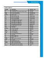
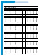
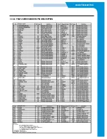
<1> Assignment of Port PAX
• PA1
: ANSWER LED (RED)
• PA2
: INK_SAVE LED (GREEN)
• PA3
: NIGHT_MODE LED (GREEN)
• PA4
: RESERVED
• PA5
: SRESERVED
• PA6
: RESERVED
• PA7
: RESERVED
* HIGH --> LED OFF
LOW --> LED ON
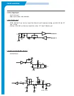
<2> Assignment of port PBX
• PB0(Output)
: LCD Enable
• PB1(Output)
: LCD R/W
• PB2(Output)
: LCD RS
• PB3(Input)
: GND
• PB4(Input)
: Unused (Pull-up)
• PB5(Input)
: GND
• PB6(Output)
: UART TXD in Main UART
• PB7(Input)
: UART RXD from Main UART
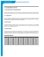
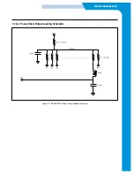
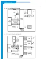
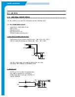
LCD ON/OFF
In case of VCC applied to LCD No. 3 PIN (BACKGROUND LEVEL), all the LCD screen will be erased. When the power is
applied, MICOM PA0~7 are Default High LEVEL, so LCD will be OFF. From Jupiter3, LCD will be ON simultaneously with OPE
reset.
Q1, Q2 have the function of simply doing On/off only.
When pressing the Power Key, actual power is not turned Off but 11.75V terminal of Thundervolt Off in the Main, while simply
the LCD DISPLAY should not appear in OPE. At this point, Micom should be operated normally to recognize the Key when
pressing the Power key again. [The same effect as Power save]
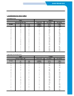
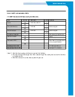
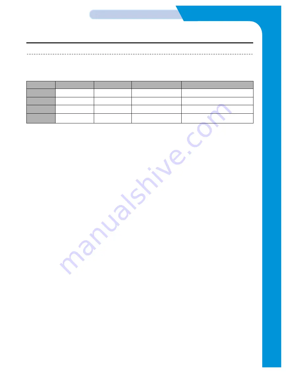
Type
I/O Control
I/O direction
USE
Remarks
PA X
Byte Control
I/O => Output
LED Control
Used as LCD VCCCONTROL in MAGIC.
PB X
Byte Control
In : 4, Out : 4
UART, LCD, Sensor
MAGIC SENSOR not applied.
PC X
Byte Control
I/O => Input
Key Input
PD X
Byte Control
I/O => Output
LCD Data, Key Scan
Summary of Contents for SF-335T
Page 2: ......
Page 19: ...CIRCUIT DESCRIPTION 2 Chorus 2 Assigned GPO Ports for RHINE ...
Page 21: ...CIRCUIT DESCRIPTION 5 HP IMPORTANT ASIC Ports for RHINE ...
Page 24: ...CIRCUIT DESCRIPTION 3 1 5 3 Block Diagram Figure 16 Block Diagram of IP_TOP ...
Page 35: ...CIRCUIT DESCRIPTION 3 1 8 6 FM214 MODEM BLOCK DIAGRAM 3 1 8 7 FM214 VS MODEM BLOCK DIAGRAM ...
Page 36: ...CIRCUIT DESCRIPTION 3 1 8 8 FM214 SERIES MODEM PIN DESCRIPTION ...
Page 48: ...4 5 Samsung Electronics SCHEMATIC DIAGRAMS Repair Manual 4 2 LIU Circuit Diagram 2002 06 25 ...