background image

4-6

SCHEMATIC DIAGRAMS

Samsung Electronics

Repair Manual

4-3 OPE Circuit Diagram

2002.06.03

D2

D6

D4

D2

D0

D0

D6

D4

Summary of Contents for SF-335T

Page 1: ...Repair Manual 1 Block Diagram 2 Connection Diagram 3 Circuit Description 4 Schematic Diagrams SAMSUNG FACSIMILE SF 330 331P 335T C O N T E N T S ...

Page 2: ......

Page 3: ...sung Electronics Digital Printing CS Group Copyright c 2002 07 This manual is made and described centering around circuit diagram and circuit description needed in the repair center in the form of appendix ...

Page 4: ...EM FM214 SF 330 331P FM214 VS SF 335T 14 4k FLASH MEMORY 8Mbit ERTE SDRAM 16Mbit SF 330 331P 64Mbit SF 335T QUARTER HORSE C DC DC CONVERT R LF SS MOTOR DRV Scecon SPEECH MAIN OPE LIU SPEAKER Encorder Sensor CR HOOK S W Ph oto SF 330 331P ONLY Interr uptor EXT LINE TEL LINE HANDSET AFE Mic SF 335T ONLY USB SF 331P ONLY SCAN MOTOR DRV TRANS 600 600 MAIN PCB 275 x 67 5mm OPE PCB 247 x 95 5mm LIU PCB ...

Page 5: ... 10 11 12 13 14 1 1 2 3 4 5 6 7 8 9 10 11 12 13 14 DGND 5V VD LCD_RW LCD_CS D0 D1 D2 D3 D4 D5 D6 D7 LCD_RS D_DET D_SCAN OPE_TXD nOPE_RST OPE_RXD 5V 1 2 3 4 5 6 7 3 2 DGND 1 2 3 4 5 6 7 AGND MIC_IN 1 2 3 4 5 6 7 8 9 10 11 12 13 14 15 16 17 18 19 20 21 22 23 24 25 26 27 28 29 30 HS_VOL_CTL AGC HS_TX_CTL AGND MODEM_RX AGND MODEM_TX DGND 5V MIC_IN CIS_SIG 1 2 3 4 5 6 7 8 9 10 11 12 13 14 15 16 17 18 1...

Page 6: ...e same as those listed in the circuit diagram 3 1 2 MEMORY MAP The entire Addressing area provided by MAIN CONTROLLER S3C46Q0X is 256MBytes from 0x00000000 to 0x10000000 and the Max Address Range for each External Chip Select is 32M Byte or Half word from 0x000000 to 0x01FFFFFF and embodied with Big Endian Bus interface MEMORY area is divided into EXTERNAL ROM and RAM areas See Figure 1 and the ar...

Page 7: ...ge of frequency being input in case of using X tal is limited to 4MHz 10MHz For making the MCLK the Clock is supplied to the EXTCLK Terminal of the ASIC by sending output power 32 256MHz of the MODEM FM214 or FM214 VS U16 XCLK via the RC Filter The inner side of the ASIC takes the Clock and it goes to the MPLL circuit to create a basic operating frequency 66MHz MCLK signal Also the Clock goes to t...

Page 8: ... SF 330 SF331P SF 335T 0 11 0 12 TX_A CIS_LED CIS_CLK CIS_CIG CIS_SI _RD _WR MODEM_RST MODEM_MCS MODEM_MIRQ OPE_TXD OPE_RXD OPE_RST TX_nA TX_B TX_nB U2 U12 U16 3 3V U10 SF 331P ONLY 1 8V U13 _scs0 LF MOTOR SS MOTOR TX MOTOR SIX SHOOTER CR_MOT_P CR_MOT_M SS A SS nA SS B SS nB LF_B LF_nB LF_A LF_nA MIC SF 335T ONLY To Analog Part ...

Page 9: ...e 4 Flash Memory Write Timing EXTCLK nGCSx nGCSx ADDR tRWD tRAD Tacs tRCD nWE DATA nBEx Tacc Toch Tcah Tocs tRCD tRWD tRDD tRAD tRDH 1 EXTCLK nGCSx nGCSx ADDR tRWD tRAD Tacs tRCD nWE DATA nBEx Tacc Toch Toch Tcah Tocs tRWBED Tcos tRDD tRWBED tRCD tRWD tRDD tRAD ...

Page 10: ...CIRCUIT DESCRIPTION Figure 5 SDRAM Read Timing SCLK SCKE ADDR BA AP A10 nGCSx nSRAS nSCAS nBEx nWE DATA 1 tSAD tSAD tSCSD tSRD Trp Trcd tSCD tSBED Tcl tSWD tSDS tSDH ...

Page 11: ...CIRCUIT DESCRIPTION Figure 6 SDRAM Write Timing SCLK 1 SCKE ADDR BA AP A10 nGCSx nSRAS nSCAS nBEx nWE DATA tSAD tSAD tSCSD tSRD Trp Trcd tSWD tSDD tSDD tSBED tSCD ...

Page 12: ...CIRCUIT DESCRIPTION Figure 7 SDRAM Write Timing SCLK SCKE ADDR BA AP A10 nGCSx nSRAS nSCAS nBEx nWE DATA tSAD 1 1 HZ tSAD tSCSD tSRD tSRD tSCD tSWD tSCSD tSAD Trp Trc ...

Page 13: ...CIRCUIT DESCRIPTION Figure 8 SDRAM auto Refresh Timing SCLK SCKE ADDR BA AP A10 nGCSx nSRAS nSCAS nBEx nWE DATA tSAD 1 1 HZ tSAD tSCSD tSRD tSRD tSCD tSWD tSCSD tSAD Trp Trc ...

Page 14: ...CIRCUIT DESCRIPTION Figure 9 SDRAM Self Refresh Timing SCLK SCKE ADDR BA AP A10 nGCSx nSRAS nSCAS nBEx nWE DATA HZ tSWD HZ 1 1 1 1 1 1 1 tCKED tSAD tSAD tSCSD tSRD tSRD tSCD tSCSD tSAD tCKED Trc Trp ...

Page 15: ...That is the device supporting each USB is con nected centering on PC The device is available for Interface for the maximum of 127 USB cable is composed of total of a set of twisted pair and 2 power lines The part for implementing USB function is included in S3C46Q0X For Interface of USB pull up of 15KΩ is interfaced to the data line of high level instruments and among data lines of lower level ins...

Page 16: ...ol Part 1 General Information It drives the Inkjet Head and it controls the HA 3 0 and _STB 5 0 which control the Six Shooter The Six shooter creates the signal to drive 48 Nozzle of the HEAD The Stubby Head in the system is the Bubble type head and has 48 nozzle for the Mono and Color Printer only 48 Nozzle Head of the mono and color head receives the data by 6 bytes per1 slice The data from the ...

Page 17: ...als SMIC clock and SMID data to transmit the data It transmits 3 bytes at once and the 3 bytes mean the Device Address Data 1 and Data 2 It is transmitted from MSB to LSB The Quarter horse sends the ACK signal at the end of the each byte to confirm the transmitted data In case of no receiving ACK signal the Quarter horse_interface Logic sends the 3 bytes again Depending on the level of the SMIC an...

Page 18: ...gister is set automatically the same value is transferred for data transfer after for a while Quarter horse con trols two Stepper motors Line Feeder and Service Station and one DC Motor Carriage Motor 10 MOTOR Control Part S3C46Q0X supports two Step Motors and one DC Motor but only TX Scan Motor is used in the system The Quarter horse supports LF SS and CR MOTOR 11 S3C46QOX General Purpose I O Por...

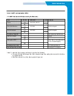
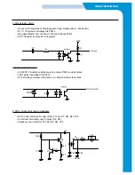
Page 19: ...CIRCUIT DESCRIPTION 2 Chorus 2 Assigned GPO Ports for RHINE ...

Page 20: ...CIRCUIT DESCRIPTION 3 Chorus 2 Assigned GPI Ports for RHINE 4 Chorus 2 Assigned GPIO Ports for RHINE ...

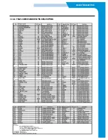
Page 21: ...CIRCUIT DESCRIPTION 5 HP IMPORTANT ASIC Ports for RHINE ...

Page 22: ... Quarter horse needs 24V to be operated but 5 0V is supplied by the Buck Regulator circuit If 5 0V is incom pletely supplied such as 4 75V it is checked as the Power Failure The _RST output becomes low 0V and the S3C46Q0X U12 confirms it to make it RESET LOW ACTIVE When the S3C46Q0X is released from RESET the _F_POR of the S3C46Q0X and FLASH MEMORY are reset 1 WATCH DOG OUTPUT _F_POR Since WATCH D...

Page 23: ... each 8 bits RGB Mono Gray Image 8 bits pixel Maximum processing Width A4 600 dpi 5KB Effective pixel Ideal MSLT Minimum Scan Line Time Grey mode Color 3 RGB X 5KB X 15nsec X 16clock 3 69 msec Grey mode mono 1 X 5KB X 15nsec X 16clock 1 23 msec Grey mode Color 1 X 5KB X 15nsec X 16clock 1 23 msec A D conversion depth 10 bits 3 1 4 1 General description MEMORY applied in this system are FLASH MEMOR...

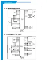
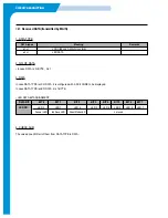
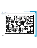
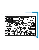
Page 24: ...CIRCUIT DESCRIPTION 3 1 5 3 Block Diagram Figure 16 Block Diagram of IP_TOP ...

Page 25: ...port which interfaces with the main controller Linear Pre regulator Circuit Power On Reset Generation Circuit and Motor Drive part 1 SERIAL INTERFACE It interfaces with the Main Controller S3C46Q0X and consists of SMIC SMID PWM and _RST Please refer to the picture 17 for the timing Figure 17 SERIAL INTERFACE INPUT timing diagram ...

Page 26: ...r phase B drive power open drain nSnB Service station motor phase nB drive power open drain DATA Serial Data Input and ACK output CMOS input SCLK Serial Clock Input CMOS input GATE1 V1 gate drive power output SOURCE1 V1 source voltage return analog input Vfb V1 return to close loop analog input COMP1 V1 compensation pin analog SWITCH 5V switching output power output COMP5 5V compensation pin analo...

Page 27: ...Reset of the Quarter horse starts to work when the 5V is going down under 4 75V It has the 1 5 5 usec of Sensitivity Timing Margin for preventing the minute shakiness of the power by ESD Also the Time Delay of the Reset can be controlled from 1ms to 1s by the Capacitor when power on 4 MOTOR DRIVERS The Quarter horse drives one DC Motor and two stepping motors The DC Motor drives 19 2V as the FULL ...

Page 28: ...ff 0 1 1 1 off off 1 0 0 0 off off 1 0 0 1 off off 1 0 1 0 on off 1 0 1 1 off on 1 1 0 0 off on 1 1 0 1 on off 1 1 1 0 off off 1 1 1 1 off off Inputs Outputs Whinny Register Bits Pin 38 37 Pin 36 32 Pin 34 30 PPWM sa sna SPWMA nSA nSnA sb snb SPWMB nSB nSnB 0 0 0 0 off off 0 0 0 1 off off 0 0 1 0 on off 0 0 1 1 off on 0 1 0 0 off on 0 1 0 1 on off 0 1 1 0 off off 0 1 1 1 off off 1 0 0 0 off off 1 ...

Page 29: ...CIRCUIT DESCRIPTION 5 Quarterhorse Block Diagram Figure 18 Quarterhorse Block Diagram showing typical external components ...

Page 30: ...for operating the Ballast Resistor and TIJ 2 0 Inkjet Head and it has 4 head address HA 3 0 input of the 6 strobe nSTB 5 0 and output of the 48 nozzle control 3 1 6 2 OPERATE TIMING AND INTERNAL BLOCK DIAGRAM figure 19 SIXSHOOTER Power Driver Driver Diagram figure 20 SIXSHOOTER inside Block diagram ...

Page 31: ... X R24 0 0 X 0 1 X X X 0 X X R30 0 0 X 1 0 X X X 0 X X R32 0 0 X 1 1 X X X 0 X X R34 0 1 X 0 0 X X X 0 X X R18 0 1 X 0 1 X X X 0 X X R20 0 1 X 1 0 X X X 0 X X R22 0 1 X 1 1 X X X 0 X X R28 0 X 0 0 0 X X 0 X X X R25 0 X 0 0 1 X X 0 X X X R3 0 X 0 1 0 X X 0 X X X R5 0 X 0 1 1 X X 0 X X X R7 0 X 1 0 0 X X 0 X X X R9 0 X 1 0 1 X X 0 X X X R11 0 X 1 1 0 X X 0 X X X R13 0 X 1 1 1 X X 0 X X X R15 0 0 X 0...

Page 32: ...CIRCUIT DESCRIPTION 3 1 6 4 Power Driver Output Loading Schematic Figure 21 SIXSHOOTER Power Output Loading Schematic ...

Page 33: ... 2V and consists of three functional blocks such as the Head the Pen ID which find out the kind of head by checking temperature and resistance difference when firing and the Resistor Test which checks the possibili ty of the head firing 3 1 7 2 ERTE Block Diagram Figure 22 Block Diagram of ERTE ...

Page 34: ..._MCS PIN 91 is a signal of the Modem Chip and _RD PIN 92 and _WR PIN 90 are control signals for a reading and writing IRQ PIN 108 is a signal for the Modem Interrupt Output The transmitting speed of the FM214 is Maximum 14 4k bps 3 1 8 3 SENDING PART The circuit manages the sending output which is analog signal of the modem The output signal by each mode comes out from the modem lineout PIN69 and ...

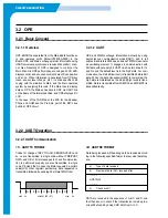
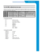
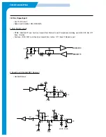
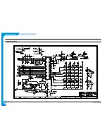
Page 35: ...CIRCUIT DESCRIPTION 3 1 8 6 FM214 MODEM BLOCK DIAGRAM 3 1 8 7 FM214 VS MODEM BLOCK DIAGRAM ...

Page 36: ...CIRCUIT DESCRIPTION 3 1 8 8 FM214 SERIES MODEM PIN DESCRIPTION ...

Page 37: ...sonator as oscillating element It engages in communication with 8bit data without parity bit UART line has two lines for Tx and Rx and the default level is in the high state For com munication the start bit low level is transmitted before 8bit data When the data transmission 8bit is completed the high state is maintained as the stop bit high level is trans mitted Data is transmitted from LSB DO an...

Page 38: ...data requested it goes out Types STATUS USED PORT LEVEL REMARKS key data ON PORT PC0 PORT PC7 L OFF H SCAN POSITION sensor ON PORT PB3 H MAGIC not applied OFF L DOC detector sensor ON PORT PB 5 L MAGIC not applied OFF H For initial use of initial OPE After power on generated only once UART communication OK Note 2 ERR LCD interface of OPE OK When failed in the interface once when succeeded first No...

Page 39: ...o be displayed In case DATA TYPE is LED DATA it is 1 BYTE LED DATA BIT ASSIGNMENT 4 CHECK SUM The value done XOR all of them from DATA TYPE to DATA DATA BIT BIT 0 BIT 1 BIT 2 BIT 3 BIT 4 BIT 5 BIT 6 BIT 7 LED NO LED 0 LED 1 LED 2 LED 3 LED 4 LED 5 LED 6 LED 7 Answer LED Ink Save LED Silent Mode LED not used DATA types Meaning Remarks a1 H LCD DISPLAY DATA FULL LINE a4 H LED DATA ...

Page 40: ... UART PB7 Input UART RXD from Main UART LCD ON OFF In case of VCC applied to LCD No 3 PIN BACKGROUND LEVEL all the LCD screen will be erased When the power is applied MICOM PA0 7 are Default High LEVEL so LCD will be OFF From Jupiter3 LCD will be ON simultaneously with OPE reset Q1 Q2 have the function of simply doing On off only When pressing the Power Key actual power is not turned Off but 11 75...

Page 41: ...tection circuit ARR1 component is the protection of lightning surge Spec 400V 20 500A VAR2 is a varistor that decrease over voltage noise Spec 82V 1250A Over 400V of high voltage is decreased by ARR1 and the rest voltage low voltage 400V under level is decreased by VAR2 2 Remote circuit C8 R13 use for DC coupling On hook impedance Over voltage is depressed by ZD component DTMF Detector path for Lo...

Page 42: ...Ext hook detector circuit SF 330 331P model have Ext phone jack to connect TAM or external phone VAR1 protect overvoltage into PC814 R7 is marching component of Ext phone for detect another normal phone 5 DCR Current limit circuit impedance DCR Current limit circuit consist of R25 C13 Q2 Q3 R21 R23 R14 Current limit circuit apply only EU nation Q3 R21 Impedance circuit consist of T2 C26 R43 R41 C3...

Page 43: ...impedance matching part R43 C35 R4 T1 trans tel line Dial tone ICM 335T and Fax tone transmit form tel line T1 trans Modem rx part 2 Speech part Handset MIC Receive Handset Receive MODEM TX MODEM RX R41 C35 R43 C26 ZD3 AGND T2 VDD VDD R27 C21 R24 AGND Q5 C17 C10 Q2 BD2 RVC R31 C23 C20 R16 C38 R26 Q4 R22 R28 VDD VDD VDD BD1 C14 R20 C16 MIC AGND AGND AGND AGND AGND ...

Page 44: ...ronics SCHEMATIC DIAGRAMS Repair Manual Samsung Electronics SCHEMATIC DIAGRAMS Repair Manual 4 Schematic Diagrams 4 1 Main Circuit Diagram 1 4 Bead 2012 type SF 330 335T 0ohm 2012 type BD5 BD8 600ohm BD6 7 120ohm SF 331P ...

Page 45: ...4 2 SCHEMATIC DIAGRAMS Samsung Electronics Repair Manual Main Circuit Diagram 2 4 FOR SF 335T 64M FOR SF 330 16M ...

Page 46: ...msung Electronics SCHEMATIC DIAGRAMS Repair Manual Main Circuit Diagram 3 4 DSP_D FM214 for SF 330 SF331P DSP_D for SF 335T FOR SF 335T DSP_D IA_D IA_A DSP_D IA_D DSP_A DSP_D FOR SF 335T FOR SF 330 DSP_D IA_A ...

Page 47: ...4 4 SCHEMATIC DIAGRAMS Samsung Electronics Repair Manual Main Circuit Diagram 4 4 ONLY 331P ONLY 331P ONLY 331P ONLY 331P ERTE ONLY 331P ...

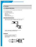
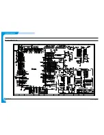
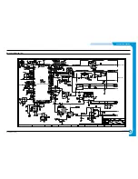
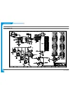
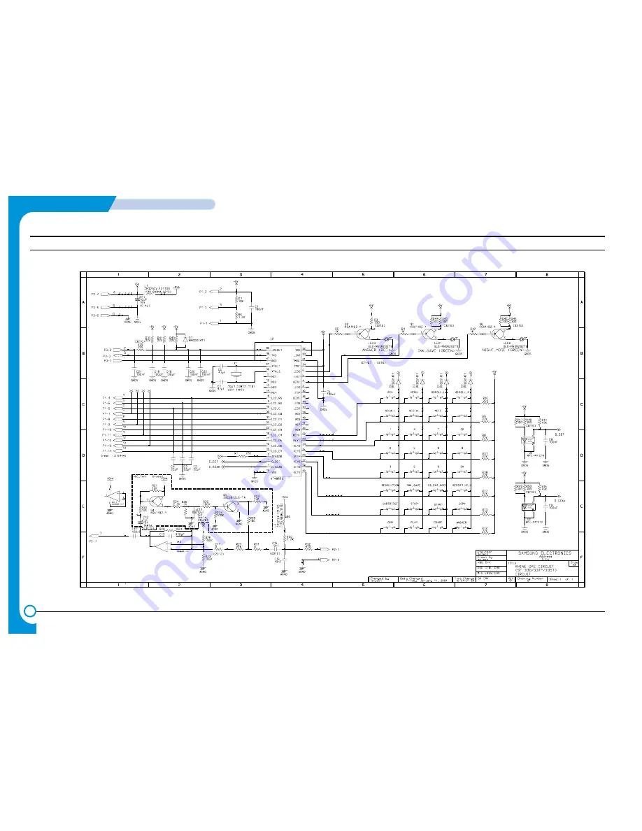
Page 48: ...4 5 Samsung Electronics SCHEMATIC DIAGRAMS Repair Manual 4 2 LIU Circuit Diagram 2002 06 25 ...

Page 49: ...4 6 SCHEMATIC DIAGRAMS Samsung Electronics Repair Manual 4 3 OPE Circuit Diagram 2002 06 03 D2 D6 D4 D2 D0 D0 D6 D4 ...

Reviews: