3-13
Samsung Electronics
CIRCUIT DESCRIPTION
Repair Manual
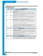
Label
I/O Type
Signal Name/Description
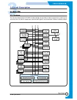
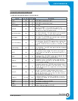
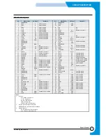
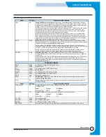
REFERENCE SIGNALS AND MODEM INTERCONNECT
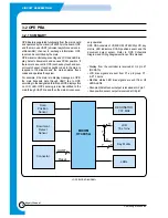
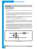
VC
MI
Low Voltage Reference. Connect to analog ground through 10 F (polarized, + terminal to VC)
and 0.1 F (ceramic) in parallel.
VREF
MI
High Voltage Reference. Connect to VC through 10 F (polarized, + terminal to VREF) and 0.1 F
(ceramic) in parallel.
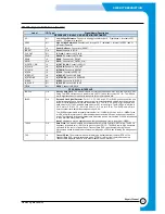
/POR
IA
Power-On-Reset. Connects to /RESET.
/RESET
OA
Reset. Connects to /POR.
CLK_OUT
MI
IA Clock. Connect to M_CLKIN.
SR4OUT
OA
SR4OUT. Connect to M_TXSIN.
SR4IN
IA
SR4IN. Connect to M_RXOUT.
SR1IO
OA
SR1IO. Connect to M_CNTRL_SIN.
M_CNTRL_SIN
IA
M_CNTRL_SIN. Connect to SR1IO.
M_CLKIN
IA
M_CLKIN. Connect to CLK_OUT.
M_TXSIN
IA
M_TXSIN. Connect to SR4OUT.
M_SCK
IA
M_SCK. Connect to EYECLK.
M_RXOUT
IA
M_RXOUT. Connect to SR4IN.
M_STROBE
IA
M_STROBE. Connect to EYESYNC.
SLEEP
MI
SLEEP. Connect to IA_SLEEP.
IA_SLEEP
MI
IA_SLEEP. Connect to SLEEP
GPO0
MI
GPO0. Connect to /RDCLK.
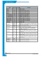
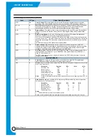
DTE SERIAL INTERFACE
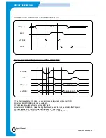
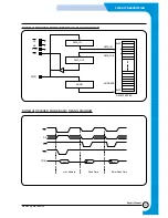
/RDCLK
OA
Receive Data Clock. The modem outputs a synchronous Receive Data Clock (/RDCLK) for USRT
timing. The /RDCLK frequency is the data rate (–0.01%) with a duty cycle of 50 –1%. The /RDCLK
low-to-high transitions coincide with the center of the received data bits.
/RLSD
OA
Received Line Signal Detector. For V.17, V.33, V.29, and V.27 ter; RLSD goes active at the end
of the training sequence. If energy is above the turn-on threshold and training is not detected, the
/RLSD off-to-on response time is 816 baud times for V.17/V.33, V.29, and V.27 ter long train; 492
baud times for V.17/V.33; and 486 baud times for V.27 ter short train. The /RLSD on-to-off time is
40 – 5 ms for V.17/V.33, 35 – 5 ms for V.29 or 11.6 – 5 ms for V.27 ter. The /RLSD on-to-off time
ensures that all valid data bits have appeared on RXD.
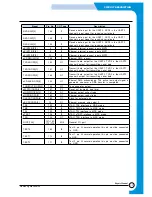
The /RLSD programmable threshold levels default to —43 dBm for off-to-on and to —48
dBm for on-
to-off. A minimum hysteresis of 2 dBm exists between the actual off-to-on and on-to-off transition
levels. The threshold level and hysteresis are measured with an unmodulated 2100 Hz tone applied
to the Receiver Analog (RXA) input.
Note: Performance may be degraded when the received signal level is less than —43
dBm.
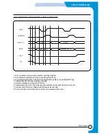
TDCLK
OA
Data Clock. The modem outputs a synchronous Data Clock (DCLK) for USRT timing. The DCLK
frequency is the data rate (–0.01%) with a duty cycle of 50 –1%. The DCLK low-to-high transitions
coincide with the center of the data bits. Transmit Data (TXD) must be stable during the one
microsecond period immediately preceding the rising edge of DCLK and following the rising edge of
DCLK.
TXD
IA
Transmit Data. The modem obtains serial data to be transmitted from the local DTE on the
Transmit Data (TXD) input in serial data mode (TPDM bit = 0), or from the interface memory
Transmit Data Register (TBUFFER) in parallel data mode (TPDM bit = 1).
FM336 Signals Definitions (Cont’d)
Summary of Contents for SF-530 Series
Page 87: ...Electronics ...

