3-14
CIRCUIT DESCRIPTION
Samsung Electronics
Repair Manual
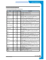
Label
I/O Type
Signal Name/Description
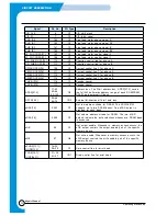
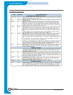
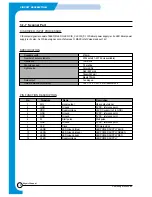
/CTS
OA
Clear To Send. /CTS active indicates to the local DTE that the modem will transmit any data
present on TXD. /CTS response times from an active condition of /RTS are shown in Tabl e 1-3.
XTCLK
IA
External Transmit Clock. In synchronous communication, an external transmit data clock can be
connected to the modem XTCLK input. The clock supplied at XTCLK must exhibit the same
characteristics as TDCLK. The XTCLK input is then reflected at the TDCLK output.
RXD
OA
Received Data. The modem presents received serial data to the local DTE on the Received Data
(RXD) output and to the interface memory Receive Data Register (DBUFFER) in parallel data
mode.
/DTR
IA
Data Terminal Ready. In V.8 and V.34 configuration, activating /DTR initiates the handshake
sequence. The DATA bit must be set to complete the handshake.
In V.21 or V.23 configuration, activating /DTR causes the modem to enter the data state provided
that the DATA bit is a 1. If in answer mode, the modem immediately sends answer tone. During the
data mode, deactivating /DTR causes the transmitter and receiver to turn off and return to the idle
state.
The /DTR input and the /DTR control bit are logically ORed.
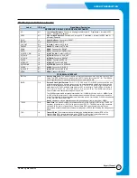
/DSR
OA
Data Set Ready. DSR ON indicates that the modem is in the data transfer state. DSR OFF
indicates that the DTE is to disregard all signals appearing on the interchange circuits except Ring
Indicator (/RI). /DSR is OFF when the modem is in a test mode (local analog or remote digital
loopback). The /DSR status bit reflects the state of the /DSR output.
/RTS
IA
Request to Send. The active low /RTS input allows the modem to transmit data present at TXD in
the serial data mode (TPDM bit = 0), or in DBUFFER in the parallel data mode (TPDM bit = 1),
when /CTS becomes active.
The /RTS hardware control input is logically ORed with the /RTSP bit by the modem to form the
resultant control signal.
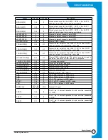
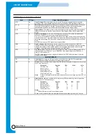
HOST INTERFACE
/CS
IA
Chip Select. The active low /CS input selects and enables the modem DSP for parallel data
transfer between the DSP and the host over the microprocessor bus.
/WR
IA
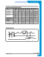
Write. Writing is controlled by the host pulsing /WR input low during the microprocessor bus access
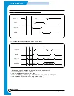
cycle. The write timing is:
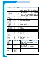
Parameter
Symbol
Min.
Max.
Units
CS Setup Time
TCS
0
—
ns
RSi Setup Time
TRS
10
—
ns
Control Hold Time
THC
10
—
ns
Write Data Setup Time
TWDS
20
—
ns
Write Data Hold Time
TDHW
10
—
ns
Note:
A read or write operation following a write operation must be delayed by at least 4 XCLK
cycles.
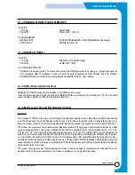
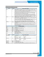
/RD
IA
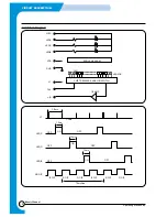
Read Enable. Reading is controlled by the host pulsing /RD input low during the microprocessor
bus access cycle. The read timing is:
Parameter
Symbol
Min.
Max.
Units
CS Setup Time
TCS
0
—
ns
RSi Setup Time
TRS
10
—
ns
Data Access Time
TDA
—
45
ns
Data Hold Time
TDHR
10
—
ns
Control Hold Time
THC
10
—
ns
Notes:
1.
/CS and /RD must not both be continuously active.
A read or write operation following a read operation must be delayed by at least 2 XCLK cycle.
FM336 Signals Definitions (Cont’d)
Summary of Contents for SF-530 Series
Page 87: ...Electronics ...

