3-15
Samsung Electronics
CIRCUIT DESCRIPTION
Repair Manual
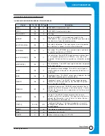
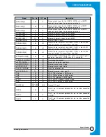
Label
I/O Type
Signal Name/Description
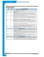
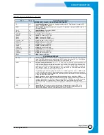
IRQ
OA
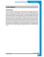
Interrupt Request. Interrupt request outputs may be connected to the host processor interrupt
request input in order to interrupt host program execution for immediate modem service. The IRQ
output can be enabled in DSP interface memory to indicate immediate change of conditions in the
modem. The use of IRQ is optional depending upon modem application.
The IRQ output structure is an open-drain field-effect-transistor (FET). The IRQ output can be wire-
ORed with other IRQ lines in the application system. Any of these sources can drive the host
interrupt input low, and the host interrupt servicing process normally continues until all interrupt
requests have been serviced (all IRQ lines have returned high).
Because of the open-drain structure of IRQ#, an external pull-up resistor to +3.3V is required at
some point on the IRQ line. The resistor value should be small enough to pull the IRQ line high
when all IRQ drivers are off (it must overcome the leakage currents). The resistor value should be
large enough to limit the driver sink current to a level acceptable to each driver. If only the modem
IRQ# output is used, a resistor value of 5.6K ohms, 20%, 0.25 W, is sufficient.
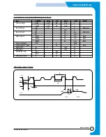
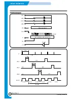
D0-D7
IA/OB
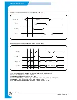
Data Lines. Eight bi-directional data lines (D0—D7) provide parallel transfer of data between the
host and the modem. The most significant bit is D7. Data direction is controlled by the Read Enable
(READ#-¿2) and Write Enable (WRITE#-R/W#) signals.
During a read cycle, data from the DSP interface memory register is gated onto the data bus via
three-state drivers in the DSP. These drivers force the data lines high for a one bit, or low for a zero
bit. When not read, the three-state drivers assume their high-impedance (off) state.
During a write cycle, data from the data bus is copied into the selected DSP interface memory
register, with high and low bus levels representing one and zero bit states, respectively.
RS0-RS4
IA/OB
Register Select Lines. Five active high Register Select inputs (RS0—RS4) address interface
memory registers within the DSP when /CS is low. These lines are typically connected to address
lines A0-A4.
When selected by /CS low, the DSP decodes RS0 through RS4 to address one of 32 8-bit internal
interface memory registers (00-1F). The most significant address bit is RS4 while the least
significant address bit is RS0. The selected register can be read from, or written into, via the 8-bit
parallel data bus (D0—D7).
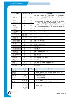
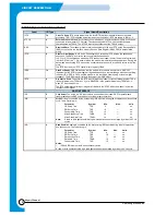
OVERHEAD SIGNALS
VDD1
PWR
3.3V Supply Voltage for DSP Digital Circuits.
VSS
DGND
Digital ground.
VGG
PWR
5V Supply Voltage for DSP Digital Circuits.
MAVSS
AGND
Analog ground.
MAVDD
PWR
5V Supply Voltage for IA Analog Circuits.
VDD
PWR
5V Supply Voltage for IA Digital Circuits.
VSUB
GND
Connect to analog ground.
XCLK
OA
XCLK Output. Output clock at 63.5045 MHz, which runs during normal operational mode and
turned off during Sleep Mode.
YCLK
OA
YCLK. Output clock at 28.224 MHz, which runs during normal operational mode and turned off
during Sleep Mode..
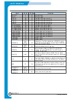
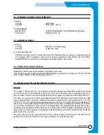
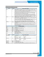
Label
I/O Type
Signal Name/Description
XTALI/CLKIN
I/O
Crystal In/Clock In. Connect to an external 28.224 MHz crystal circuit or an external 28.224 MHz
oscillator circuit.
Label
Crystal
Oscillator
XTALI/CLKIN
XTALI
CLKIN
XTALO/NC
I/O
Crystal Out/NC. Connect to the external crystal circuit return or leave open.
Label
Crystal
Oscillator
XTALO/NC
XTALO
NC
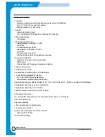
PLL_VDD
PWR
PLL Supply Voltage.
PLL_GND
DGND
PLL Supply Voltage return.
VCORE
PWR
3.3V Supply Voltage. Connect to VDD1.
RESERVED
-
Reserved pins are used for future development and should not be connected to any circuitry.
FM336 Signals Definitions (Cont’d)
Summary of Contents for SF-530 Series
Page 87: ...Electronics ...

