3-5
Samsung Electronics
CIRCUIT DESCRIPTION
Repair Manual
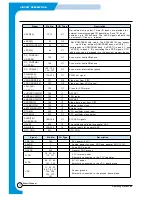
Signal
Pin No.
I/O Type
Description
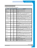
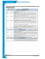
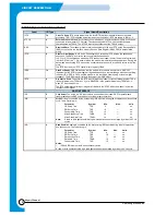
RXD0/GIP[0]
194
I1
Receive data input for the UART0. RXD0 is the UART0
channel's input signal for receiving serial data.
RXD1/GIP[1]
192
I1
Receive data input for the UART1. RXD1 is the UART1
channel's input signal for receiving serial data.
RXD2/GIP[2]
190
I1
Receive data input for the UART2. RXD2 is the UART2
channel's input signal for receiving serial data.
nEINT0/GIP[3]
8
I3
External interrupt request input nEINT0.
nEINT1/GIP[4]
9
I3
External interrupt request input nEINT1.
nEINT2/GIP[5]
10
I3
External interrupt request input nEINT2.
nXDREQ/GIP[6]
199
I3
External DMA request.
TXD0/GOPA[0]
193
O1
Transmit data output for the UART0. TXD0 is the UART0
channel's output for transmitting serial data.
TXD1/GOPA[1]
191
O1
Transmit data output for the UART1. TXD1 is the UART1
channel's output for transmitting serial data.
TXD2/GOPA[2]
189
O1
Transmit data output for the UART2. TXD2 is the UART2
channel's output for transmitting serial data.
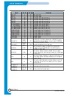
nXDACK/GOPA[5]
200
O1
External DMA acknowledge. This active low output signal is
generated whenever a DMA transfer is completed.
TONEOUT/GOPA[3]
188
O1
Tone generator output.
nWDTO/GOPA[4]
187
P3
Reset out by watch dog timer.
nIOWR/GOPA[10]
161
O1
External output write strobe
nIORD/GOPA[9]
162
O1
External output read strobe
CLKOUT/GOPA[6]
180
O1
Clock for external chip
nECS2/GOPA[8]
14
O1
External memory chip select 2.
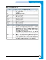
TCK
132
I2
JTAG TCK interface in MDS mode.
TMS
135
I2
JTAG TMS interface in MDS mode.
TDI
133
I2
JTAG TDI interface in MDS mode.
nTRST
136
I2
JTAG nTRST interface in MDS mode.
TDO
134
O1
JTAG TDO interface in MDS mode.
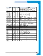
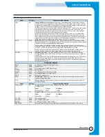
GIOP[10:0]
137~140,
173~179
I/O4
General I/O port.
TEST0
169
I2
Test 0 pin. At normal operation this pin must be connected
to
GND.
TEST1
170
I2
Test 1 pin. At normal operation this pin must be connected
to GND.
TEST2
171
I2
Test 2 pin. At normal operation this pin must be connected
to
GND.
Summary of Contents for SF-530 Series
Page 87: ...Electronics ...

