background image


Digital Laser MFP


SF-830/SF-835P


1. Precautions

2. Specifications

3. Disassembly

4. Troubleshooting

5. Exploded Views and Parts List

6. Block Diagram

7. Connection Diagram


Digital Laser MFP

Contents


SERVICE


MANUAL

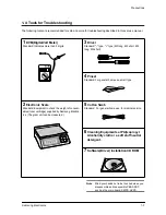
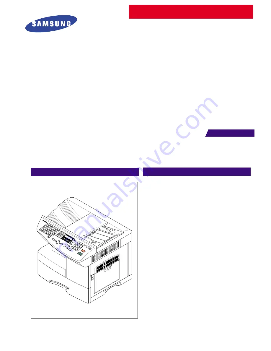
Summary of Contents for SF-830

Page 1: ...gital Laser MFP SF 830 SF 835P 1 Precautions 2 Specifications 3 Disassembly 4 Troubleshooting 5 Exploded Views and Parts List 6 Block Diagram 7 Connection Diagram Digital Laser MFP Contents SERVICE MANUAL ...

Page 2: ...TRONICS This service manual is also provided on the web the ITSELF system Samsung Electronics Co Ltd http itself sec samsung co kr Samsung Electronics Co Ltd MARCH 2002 Printed in Korea VERSION NO 1 00 CODE ...

Page 3: ... of the information in this manual are prohibited from free duplication use or translation without prior written approval except in cases allowed by the Copyright Act Specifications are subject to change without prior notice Copyright c 2002 3 Samsung Electronics Digital Printing CS Group ...

Page 4: ... Telephone page 2 4 2 8 Packaging page 2 4 2 9 Environmental Condition page 2 4 3 Disassembly and Reassembly page 3 1 3 1 General Precautions on Disassembly page 3 1 3 2 Rear Cover page 3 1 3 3 Scanner Ass y page 3 2 3 4 ADF Ass y page 3 6 3 5 OPE Ass y page 3 8 3 6 Side Cover Ass y page 3 9 3 7 Fuser Ass y page 3 11 3 8 Exit Ass y page 3 12 3 9 Cover Paper Exit Ass y page 3 12 3 10 Drive Ass y pa...

Page 5: ...age 4 14 4 6 Troubleshootion page 4 15 4 6 1 Scanner page 4 15 4 6 1 1 COPY page 4 15 4 6 1 2 PC Scan page 4 16 4 6 2 FAX only SCX 5312F page 4 17 4 6 2 1 FAX TELEPHONE Precautions page 4 17 4 6 3 Print Quality page 4 18 Abnormal Image Printing and Defective Roller page 4 20 No Image page 4 21 All Black page 4 23 Vertical White Line Band page 4 24 Dark Image page 4 25 Background page 4 26 Ghost pa...

Page 6: ... 5 3 ADF ASS Y Exploded View Parts List page 5 9 5 4 Side Cover Ass y Exploded View Parts List page 5 12 5 5 Cassette Ass y Exploded View Parts List page 5 14 5 6 Exit Ass y Exploded View Parts List page 5 16 5 7 Feeder Ass y Exploded View Parts List page 5 18 5 8 MP Ass y Exploded View Parts List page 5 20 5 9 Base Frame Exploded View Parts List page 5 22 5 10 Pick up Ass y Exploded View Parts Li...

Page 7: ...ced with parts which meet the original specifications Always determine the cause of damage or overheating and correct any potential hazards 6 Observe the original lead dress especially near sharp edges AC and high voltage power sup plies Always inspect for pinched out of place or frayed wiring Do not change the spacing between components and the printed circuit board 7 Product Safety Notice Some e...

Page 8: ...charges suffi cient to damage ESDs 5 Do not use Freon propelled chemicals When sprayed these can generate electrical charges sufficient to damage ESDs 6 Do not remove a replacement ESD from its pro tective packaging until immediately before install ing it Most replacement ESDs are packaged with all leads shorted together by conductive foam aluminum foil or a comparable conductive material 7 Immedi...

Page 9: ...t Standard For general home use small type 2 Electronic Scale Standard Equipment to check the weight of consum ables toner cartridge supplied by Samsung Electron ics The gram unit can be measured 5 Cotton Swab Standard For general home use for medical service 6 Cleaning Equipments a IPA Isopropyl Alcohol dry cloth or a soft stuff neutral detergent 7 Software Driver installation CD ROM Note Mind yo...

Page 10: ...ondition Temperature 20 C 40 C Humidity 10 RH 95 RH Operating Condition Temperature 10 C 32 C Humidity 20 RH 80 RH Recommended Operating Condition Temperature 16 C 30 C Humidity 30 RH 70 RH Dimension W X D X H 560 X 433 X 459 mm Weight About 22 5 Kg with CRU Acoustic Noise Less than 56 47 dB Copy Printing mode Power Rating AC 100VAC 127VAC 15 50 60Hz 3Hz AC 220VAC 240VAC 15 50 60Hz 3Hz Power Consu...

Page 11: ... Side Out Paper Capacity Input Cassette 550 Sheets By Pass Tray 100 Sheets based on 75g ß 20lb Paper Capacity Output Face Down 250 Sheets Effective Print Width 203 1mm 8 inch Item Description Standard Recommendation ITU T Group3 ITU International Telecommunications Union Application Circuit PSTN or behind PABX PSTN Public Switched Telephone Network PABX Private Automatic Branch Exchange Data codin...

Page 12: ...ntact Image Sensor Module Interface IEEE1284 ECP Support USB without HUB Mode Compatibility TWAIN Standard WIA Optical Resolution H X V 300 X 300 dpi Halftone 256 Levels Effective Scan width 8 2 inches 208 mm Item Description Mode B W Quality Text Photo Mixed Mono Copy Speed 1 ADF MDSP Text mixed Approx 7 cpm Photo Approx 3 cpm Optical Resolution H x V 300 X 300 dpi Multi Copy 999 pages Maximum Or...

Page 13: ...on 1Touch Dial 50 EA 1 25 shift key 26 50 Speed Dial 200 EA Tone Pulse Tone only user modeTone Pulse selectable in tech mode Item Description Type Separate type Toner Cartridge Drum Cartridge Life Toner Cartridge 6 000 sheets 5 coverage pattern simplex normal mode Drum Cartridge 15 000 sheets simplex normal mode ...

Page 14: ...heir original positions Before removing any component from the machine note the cable routing that will be affected Whenever servicing the machine you must perform as follows 1 Check to verify that documents are not stored in memory 2 Unplug the power cord 3 Use a flat and clean surface 4 Replace only with authorized components 5 Do not force to remove or planten plastic material components 6 Make...

Page 15: ...3 1 2 Remove the six screws and take out the Shield Main Upper 3 Remove the three screws as shown below 4 Open the Side Cover Ass y first to open the Front Cover in the other words close the Front Cover first to assembly it 5 Unplug the one connector from the Main Board and remove two screws 6 Pull up the Scanner Ass y in the direction of arrow ...

Page 16: ...Rear Cover see page 3 1 Scanner Ass y see page 3 2 2 Remove the two screws securing the Scanner Ass y 3 Pull the OPE Ass y as shown below 4 Unplug the two connector from the OPE Ass y 5 Remove nine screws securing the OPE PBA to the OPE Cover 6 Remove the Contact Rubber from the unit 7 Remove the Key Pad from the unit ...

Page 17: ...F Ass y you should remove Rear cover see page 3 1 Scanner Ass y see page 3 2 OPE Ass y see page 3 3 2 Open the ADF Upper Ass y 3 Remove the Ground Cable and unlatch the Link Tray from the Cover Gear as shown below 4 Remove the ADF Upper Ass y as shown below Link Tray 1 2 Cover Gear ADF Upper Ass y ...

Page 18: ...e page 3 2 OPE Ass y see page 3 3 ADF Upper Ass y see page 3 4 2 Remove the four serews securing the Guide Lower Ass y 3 Push the part to the arrow direction to the inner unlatch the part to the arrow direction and remove Guide Lower Ass y 4 Pull the Input Tray and remove it 5 Take out the Housing Upper ADF as shown below Guide Lower Ass y 1 2 Input Tray Housing Upper ADF ...

Page 19: ...er Ass y see page 3 4 Guide Lower Ass y see page 3 5 2 Unplug the two connectors and FFC Cable from the Scan Board 3 Remove the seven screws securing the ADF Lower Ass y 4 Unlatch the Exit Roller gear part and remove it as shown below 5 Unlatch the Scan Roller gear part and remove it as shown below 6 Unlatch the ADF Roller gear part and remove it as shown below FFC Cable Exit Roller 2 1 Scan Rolle...

Page 20: ...ull the CIS Cable Take out the CIS Ass y 9 Remove the one screw securing the CIS Bracket and take out the CIS 10 Remove the four screws securing the ETC Motor Ass y and remove it 11 Unlatch the Cover Switch and remove it as shown below 12 Unlatch the both side and remove the Scan Board Pick up Roller CIS Ass y CIS Bracket CIS 1 2 Cover Switch 1 2 ...

Page 21: ...nd after pull the part to the arrow direction to the top pull the part to the arrow direction inner side 1 2 3 MP Tray 1 Pull the both side of the part to dissemble it 2 As the part make the Tray Case and the Tray Link in rectangular position to dissemble the Tray Case from the Tray Link The Tray Link locates at an angle of 45 from the Side Cover Ass y and then remove the Tray Link Tray Link Tray ...

Page 22: ...onics 3 9 Duplex Ass y 1 Unite the part and home to the projection part of the Side Cover assembly and widen them from each other to dissemble the Side Cover Ass y DeplexAss y Transfer Roller Ass y 1 Take out the Transfer Roller as shown below ...

Page 23: ...screw and take out the Cover Sheet Connector 3 Unplug the one connector 4 Remove the three screws and take out the Fuser Ass y 6 Remove the two screws and take out the Halo gen Lamp 5 Remove the four screws and take out the Ther mostat 7 After remove the two screw and open the Lower Ass y froward tack out the Heat Roller Ass y from Upper Fuser Ass y Halogen Lamp Thermostat Heat Roller ...

Page 24: ...Ass y you should remove Rear Cover see page 3 1 Scanner Ass y see page 3 2 Side Cover Ass y see page 3 8 2 Take out the Cover rr Ass y as shown below 3 Remove three screws unplug four connectors and unlatch the Dummy Base Frame as shown below 4 Pull the Exit Ass y and remove it Cover Rear Ass y ...

Page 25: ... Electronics 3 11 Cover Paper Exit Ass y 1 Before you remove the Cover Paper Exit Ass y you should remove Rear Cover see page 3 1 Scanner Ass y see page3 2 2 Remove two screws and Cover Paper Exit Ass y as shown below Cover Paper Exit Ass y ...

Page 26: ... the Drive Ass y you should remove Rear Cover see page 3 1 Shield Main Upper see page 3 2 2 Unplug the two connectors Main Motor 9pin Duplex Solenoid 2pin 3 Remove the one screw and take out the Fan and Dust Fan 4 Remove the five screws and take out the Drive Ass y Fan Dust Fan Drive Ass y ...

Page 27: ...SU youshould remove Rear Cover see page 3 1 Scanner Ass y see page 3 2 Side Cover Ass y see page 3 8 Exit Ass y see page 3 11 Cover Paper Exit Ass y see page 3 11 2 Remove three screws and take out the Shield SMPS Upper 3 Unplug the all connectors 4 Remove the SMPS as shown below SMPS ...

Page 28: ...nics 3 15 3 14 LSU 1 BeforeyouremovetheLSU youshould remove Rear Cover see page 3 1 Scanner Ass y see page 3 2 Side Cover Ass y see page 3 8 Exit Ass y see page 3 11 2 Unplug the two connectors 3 Remove the three screws and take out the LSU LSU ...

Page 29: ...it Ass y see page 3 11 SMPS see page 3 13 LSU see page 3 14 2 Remove one screw in the Channel Base Frame from the bellow section of the Cover Dummy Lower and then remove the rest of the five screws to dissemble the Dummy Scan Lower 3 Remove the Locker Deve 4 Unplug the all connectors 5 Remove the seven screws and take out the Main Frame Ass y Dummy Base Frame Cam Jam Remove Front Cover Lock Deve C...

Page 30: ...Disassembly and Reassembly Samsung Electronics 3 17 Cover Exit Rear 1 Remove the one screw and take out the Panel Connect MPF 2 Remove the one screw and Cover Exit Rear as shown below Cover Exit Rear ...

Page 31: ...and Reassembly 3 18 Samsung Electronics MP Ass y 1 Unplug the two connectors 2 Remove the four screws and take out the Dummy Cover 3 Release the SMPS fit Pull the MP Ass y Upward and remove it Dummy Cover MP Ass y ...

Page 32: ...crews 2 Pull the Feed Ass y upward and remove it Pick Up Ass y 1 Unplug the three connectors 2 Remove the two screws and take out the Cas sette Rail 3 Remove the four screws and take out the Pick Up Ass y as shown below Feed Ass y Feed Ass y Cassette Rail Pick up Ass y Guide Paper Out ...

Page 33: ...1 Remove the two screws and take out the Shield Main Lower 2 Remove the five screws and take out the Main PBA from the Shield Main Lower 3 Remove the one screw and unlatch the LIU PBA securing the Main PBA and remove it Shield Main Lower Main PBA LIU PBA Main PBA ...

Page 34: ...he SF 835P The information about the fax function is not applied for the SF 830 The differences by each model are explained in a separate way 4 1 Preventative Maintenance The cycle period outlined below is a general guideline for maintenance The example list is for an average usage of 50 transmitted and received documents per day Environmental conditions and actual use will vary these factors The ...

Page 35: ...was not answered after all the redial attempts Try again Make sure the remote machine is OK NO NOT ASSIGNED The speed dial location you tried to use has no num ber assigned to it Dial the number manually with the keypad or assign the number NO PAPER ADD PAPER The recording paper has run out The printer system stops Load the recording paper in the paper feeder OVERHEAT The printer part has overheat...

Page 36: ...OPEN HEAT EROR Thermister does not connected to main board or con tact point is not coupled tightly in power on Check thermister contact point Heating Camp Thermostat Heating Error During operation Temperatare does not go up Check thermister contact point Heating Lamp Scanner Locked Scanner is locked by locker Check locker Connect the Flat Cable Error Message Description Solution ...

Page 37: ...AL NO FAX ANS FAX TEL RINGER VOLUME LOW HIGH 10 STEPS ALARM SOUND ON OFF KEY SOUND ON OFF SPEAKER CONTROL COM ON OFF SELECT LANGUAGE ENG GER FRE ITA SPA POR DUT FAX DUPLEX OFF LONG EDGE SHORT EDGE PAPER TYPE PLAIN PAPER BOND TRANSPAR ENCY CARD STOCK LABELS PREPRINTED COLORED ENVE LOPE MEMORY CLEAR Memu One touch05 SYSTEM ID SYSTEM DATA PHONE BOOK MEMORY TX RX JOURNAL DELAY TX Memu One touch06 MEMO...

Page 38: ...the Tech mode press MENU 1 9 3 4 in sequence and the LCD briefly displays T the machine has entered service tech mode While in Tech mode the machine still performs all normal operations To return to normal user mode press MENU 1 9 3 4 in sequence again or turn the power off then on by unplugging and plugging the power cord Options changed while in service mode do not remain changed unless you clea...

Page 39: ...uch11 The same as User Mode MAINTENANCE Memu One touch12 ADJUST SHADING CLEAN DRUM NEW DRUM NOTIFY TONER ON OFF SWITCH TEST MODEM TEST SRAM TEST DRAM TEST ROM TEST FLASH ENGINE PATTERN TEST 1 7 ALL CLEAR COUNT PASSWORD TOTAL PAGE COUNT CRU PRINTS COUNT ADF SCAN COUNT USED DRUM COUNT USED TONER COUNT ANSWER ON CNG 1 4 FLASH UPGRADE LOCAL REMOTE USER PROGRAM EMULATION BOOT PROGRAM PROGRAM DIAL 1 SET...

Page 40: ...ent from factory Never change settings arbitrarily ERROR RATE When the error rate is about to be over the setting value the Baud rate automatically lowers up to 2400 bps to make the error rate remain below the setting value You can select the rate between 5 and 10 MODEM SPEED You can set the maximum modem speed Communication is done with modem speed automatically set at lower speed when communicat...

Page 41: ...unsatisfied perform the function to check the condition of the print out for checking whether or not having CCD trouble Method 1 Select the ADJUST SHADING at the TECH MODE 2 Push the SET UP button then an image will be scanned 3 After the scan CCD SHADING PROFILE will be print out 4 If the printed image is different to the image the CCD is defect NOTICE When you test CCD make sure that the cover i...

Page 42: ... function erases information of history such as replacement times of Developing part and OPC drum total printing pages scan times and etc The items are in the below section of the System Data List printed at TECH MODE PASSWOEED 1934 Current Drum Page Count cannot be erased It is possible to erase at NEW DRUM function USER MODE MINTENANCE NEW DRUM PATTERN TEST Using this pattern printout you can ch...

Page 43: ... part of the main board is poor SWITCH TEST Use this feature to test all keys on the operation control panel The result is displayed on the LCD window each time you press a key NOTIFY TONER LOW With this feature enabled when the toner becomes low the toner low information will be sent to ta specified contact point for example the service company After you access this menu select ON and when the LC...

Page 44: ...reference guide RECEPTION This journal shows a specific information concerning reception activities the time and dates of up to 40 of the most recent receptions TRANSMISSION This journal shows a specific information concerning transmission activities the time and dates of up to 40 of the most recent transmissions SYSTEM DATA This list provides a list of the user system data settings and tech mode ...

Page 45: ...down_com bin fprt exe and Rom File file name for upgrade Save the files in the same folder b In the DOS input as below and push the enter key Then it will be automatically upgraded c There are two commands for the conditions of product When the product is in idle condition down rom file When the product is in idle condition TECH MODE MAINTENANCE FLASH UPGRADE LOCAL fprt rom file d Do not turn off ...

Page 46: ...the first Scan page count Print page count etc The time is remembered to first machine use event Method These contents are remembered continuously after memory delete Clear All Memory Method Press MENU 1 9 3 in sequence Firmware version is displayed on LCD Press 1 in the number keypad The LCD display shows Updated date Press 2 in the number keypad The LCD display shows Product first use date FLASH...

Page 47: ... Hsync Test 1 On 2 Off 3 LD On Test 1 On 2 Off 4 LSU Operation 1 On 2 Off 2 1 Feed Sensor Test Sensor On FEED SENSOR ON Display Sensor Off FEED SENSOR OFF Display 2 Exit Sensor Test Sensor On EXIT SENSOR ON Display Sensor Off EXIT SENSOR OFF Display 3 Cover Sensor Test Sensor On COVER SENSOR ON Display Sensor Off COVER SENSOR OFF Display 4 1 st CAST Empty Test Sensor On 1 st PAPER Empty Display Se...

Page 48: ...eplace Main PBA Light image 1 Check seal tape removing 2 LSU light power normal 3 Enough toner 4 High charger voltage 5 Lower bias voltage 6 Contamination of high voltage contact 7 Transfer volatge and roller 1 Check and remove tape 2 LSU light power check is difficult Compare with new one and check 3 Check toner and developer counter 4 5 Measure all high voltage output 6 Leakage toner cause bad c...

Page 49: ...3 The machine was under the low tempera ture for a long time 1 Should use recommended paper 2 Check engine controller board If you have not thermometer measure the thermistor voltage to CPU If 2 3V 5 in printing CPU works well Then disassemble fuser and check the thermistor contact and thermistor 3 Re check after putting the machine in the warm place for certain period Partial blank image not peri...

Page 50: ...stable high voltage contact 2 Charge roller s contamination 3 Contamination of heat roller 4 Malfunction of LSU 1 Clean each contact and check good contact 2 Clean charge roller 3 Replace fuser unit 4 Check Main PBA NO Roller Abnormal image period Kind of abnormal image 1 OPC Drum 94 3 mm White spot Black spot 2 Charge Roller 37 7 mm White spot Black spot 3 Supply Roller 35 8 mm Horizontal dark ba...

Page 51: ... LSU might be misplaced so the light path to the OPC deviates Repair or replace LSU or remove any defective matters in the machine Self test pattern prints No image Self testing is possible Is the OPC terminal of machine is well connected to Frame Does the video data line to LSU transit to High Low when printing Retest after replacing the connector or controller board Aon nextpage NO NO NO NO NO Y...

Page 52: ...window A Transfer voltage OK on the transfer roller shaft Are the connection terminal and connection correct Repair or replace terminal Replace HVPS or repair defective component Is the connection terminal OK Replace HVPS or repair defective component Repair or replace terminal Developing 300V and supplying 450V voltage are OK Does the counter indicate over the toner s guaranty life Replace the to...

Page 53: ...air or replace toner cartridge Does the video data line to LSU transit to High Low when printing Replace LSU Check the path among video controller engine board HVPS LSU for the shortage or open Repair or replace the boards Repair or replace HVPS Replace LSU NO NO NO NO YES YES YES YES All Black Digital Printer Digital Printer Digital Printer Digital Printer Digital Printer ...

Page 54: ...tuck to blade in the developer inside and it prevents toner supply Replace the developer Check both if the toner cartridge s counter is over its guaranty and amount of the toner material Replace the toner cartridge The ribs in fuser or toner on the roller may invoke the image problem Replace the fuser cover or the defective part The image is originally black or the black part is far close to the t...

Page 55: ... LSU Repair or replace the defective component The power of LSU is set high or internal problem Replace LSU or adjust volume Same at Normal END NO NO NO Toner over supply due to the adjustment fault of metering blade in developer Replace developer NO YES YES YES YES Dark Image Digital Printer Digital Printer Digital Printer Digital Printer Digital Printer ...

Page 56: ... developer is defective Replace the toner cartridge Check Terminals or contacts and Guide Deve Spring are misplaced Repair or replace transfer roller etc Check if the LED of PTL in front of the transfer roller is on when it presses the top cover switch on purpose If not replace PTL Print 20 to 30 pages using the recommended paper Same problem occurs Adjust voltage or replace HVPS Repair or replace...

Page 57: ...ce the terminal contacts A specific part of the transfer roller has ruined or its resistance value is changed Replace transfer roller Transfer roller cannot force regularly due to the gears eccentricity of transfer roller Replace the defective component Bias voltage is OK 300V Operating storage temperature is too low or not recommended paper used Adjust the Bias voltage or replace HVPS There may b...

Page 58: ... taking out the cartridge toner leaks Toner leaks and much toner material dropped onto the paper Replace the developer Bad image removes by scratching Check toner is stuck onto the P R or H R in fuser Clean it or replace The problem randomly occurred due to the toner fallen Clean the machine NO NO NO YES YES YES Digital Printer Digital Printer Digital Printer Digital Printer Digital Printer ...

Page 59: ...l Heat roller is ruined Replace the roller The OPC is damaged due to the irregular transfer voltage of HVPS Repair replace HVPS If the same problem persists replace the developer Does it appear at every 83mm at specific place Problems of terminal contact transfer voltage supplying and transfer roller s due to the charge roller is ruined 38mm Repair replace HVPS developer NO NO NO NO YES YES YES YE...

Page 60: ...oltage drops while printing Defective agitator in the toner supplying part of developer Replace the developer Check if the guide deve spring works OK and repair repalce Check high voltage output and repair replace terminals HVPS Replace lamp Clean the window of PTL Bad images around the no image area Irregularity of toner supply from developer Replace developer Light distortion due to the mirror r...

Page 61: ...When putting in out the developer scratch is made Replace the developer Transfer voltage is normal D R in developing unit has the defect Replace the developer Too high voltage supplied due to the setting error of transfer voltage Adjust replace HVPS NO NO YES YES White Spot Digital Printer Digital Printer Digital Printer Digital Printer Digital Printer ...

Page 62: ...n 10 films are guranteed Reduce the number of films and re insert after paper check LED if off Use the recommended film When OHP printing does the fan temporarily stops and revolves Use the recommended film Other parts are touching the fan and prevents it from revolution Check and repair NO NO NO YES YES YES Trembling at the End When OHP Print ...

Page 63: ...ng time Place the machine at normal temperature and re test While printing the voltage of pin 60 of U36 CPU on Main PBA is 2 1V 2 6V Thermistor s contact is OK Open the top cover When black printing is the fuser NIP width is 3 0 3 5mm The paper used is too thick or contains too much cotton in it Re test with the recommended paper Check if the hardness of P R and spring force is OK hardness 24 degr...

Page 64: ...6 Does not the Guide Adjust distort the papers 1 Check whether solenoid is working or not by using Engine test mode 2 Check feed sensor malfunction 3 Re try inserting a fewer papers fan the papers and align take out the loaded papers and insert them reverse direction 4 Take out the loaded papers and insert them reverse direction inserted papers as recommended for Manual Feeding When loading tap th...

Page 65: ...HVPS and change it Feeding obstacles Does the Plate knockup prevent the paper loading MPF Turn the power off and on Open and close the Side cover to return to the original state Cassette Adjust Guide to fit the paper width Skew Is the Guide adjust set to the paper width Fit the paper width using the Guide adjust Stacking 1 Took out the Stacker extender to support long papers 2 Stacked too many pap...

Page 66: ... board are OK Re connect firmly and re test The connection error between controller board and panel board or malfunction of boards Replace the boards Fuse of SMPS if open Shortage between 5V and GND or between 24V and GND Replace the fuse Toner cartridge is in the set Detect failure due to the board which detects side cover open or switch error Replace the board or switch Put in the cartridge Remo...

Page 67: ...e to the heat etc Replace the thermostat The voltage of pin 6 of U5 on the Main PBA is about 3 2V If not check the CN4 on the power board Measure the resistance at the both ends of AC Line with covers open Remove the covers Re assemble the top cover and close it Thermistor connecting point or engine board defect Repair replace the component board NO NO NO YES YES YES Fuser Error ...

Page 68: ...t Feeder sensor is assembled reverse Switch them The sensor and Main PBA defected Repair replace Too many papers in the feeder Paper guides fit the paper width Paper end curled Does the extender pulled out Recommendation Use the MPF for the thick paper such as envelope and cardstock Reduce the amount and re test Take out the paper and re insert Use the recommended and quality paper Pull out the ex...

Page 69: ... the recommended paper Check guide transfer is grounded Check the shutter prevents feeding Check the input path to the fuser such as mis assembly The actuator of paper exit sensor works OK Check the actuator exists and its operation and around the Main PBA Replace Is the paper rolled around the presseure roller Remove the fuser remove the paper and replace the pressure roller if necessary Feeds mu...

Page 70: ... Main B D CN7 9 P_MOTOR Signal Check Main B D CN7 8 LREADY Signal END Try again to connector or Replace connector Replace Main PBA Replace LSU Replace Main PBA Replace LSU NO NO NO NO NO YES YES YES YES YES Check Main B D CN7 4 LDON Signal Check Main B D CN7 1 HSYNC Signal Engine Error ...

Page 71: ...an a few minutes may cause damage to the cartridge Service for the Life of Toner Cartridge If the printed image is light due to the life of the toner you can temporarily improve the print quality by redis tributing the toner Shake the toner cartridge however you should replace the toner cartridge to solve the problem thoroughly Service for Judgement of Inferior Expendables and the Standard of Guar...

Page 72: ...f the life span 2 In case of 2 If it becomes better after cleaning the LSU window then the developer is nor mal Because of foreign substance on the LSU window the image has not been printed partly 3 In case of 3 If the cycle of noise is about 2 seconds the toner inside the developer has been nearly exhausted Purchase and replace with a new developer after using about 200 sheets at the point of occ...

Page 73: ...ace the developer at intervals of 37 7mm Remove foreign substance Clean the Charged Roller Broken image Replace the developer according to carelessness 3 In case of 3 Exchange the transfer roller because the life of the transfer roller in use has been expired Check the transfer voltage and readjust if different Recycled product Poor appearance of the developer Unclean and rough printouts Bad backg...

Page 74: ...stances are stuck to the termi nal point of contact of the developer and the state of assembly Especially check the charged roller terminal 1 All of 1 2 3 above 1 Remove toner and foreign substances adhered to the contact point of the developer 2 The contact point of the unit facing that of the developer also must be cleaned 3 If the terminal assembly is unsafe Fully stick the terminal to or reass...

Page 75: ...printer first the remove the scanner from the PC to see if the printer is prop erly working alone Check and Cause Solution 1 Secure more space of the hard disk 2 Printing error occurs even if there is enough space in the hard disk 3 Check the parallel port related items in the CMOS Setup 4 Reboot the system to print 1 Not working with the message insufficient printer memory means hard disk space p...

Page 76: ... Windows to restart printing job 3 Shut down all other programs except the current one if pos sible 4 Delete the printer driver completely and reinstall it 5 After rebooting the computer check for viruses restore the damaged files and reinstall the program to do the printing job 6 Add up enough memory to the PC Description The printing is not working properly even when the cable has no problem eve...

Page 77: ...R ASS Y JC96 02430C PMO OPE COVER JC72 00796C PCT ONETOUCH PAPER JC72 00872C PCT LCD WINDOW JC72 00870C PMO COVER DUMMY OPE JC72 00858C PBA SUB LIU JC92 SCX 5312F XEF DESCRIPTION SEC CODE ELA HOU SCANNER ASS Y JC96 02451G ELA HOU PLATEN ASS Y JC96 02429D ELA HOU OPE COVER ASS Y JC96 02430D PMO OPE COVER JC72 00796D PCT ONETOUCH PAPER JC72 00872D PCT LCD WINDOW JC72 00870D PMO COVER DUMMY OPE JC72 ...

Page 78: ... ELA HOU SCANNER ASS Y JC96 02451F ELA HOU PLATEN ASS Y JC96 02429G ELA HOU OPE COVER ASS Y JC96 02430G PMO OPE COVER JC72 00796G PCT ONETOUCH PAPER JC72 00872G PCT LCD WINDOW JC72 00870G PMO COVER DUMMY OPE JC72 00858G PBA SUB LIU JC92 SCX 5112 XEC DESCRIPTION SEC CODE ELA HOU SCANNER ASS Y SEC JC96 02447D ELA HOU PLATEN ASS Y SEC JC96 02445F ELA HOU OPE COVER ASS Y JC96 02444F PMO OPE COVER JC72...

Page 79: ... 5 6 OPE Ass y Exploded View Parts List page 5 14 5 7 Cassette Ass y Exploded View Parts List page 5 16 5 8 Exit Ass y Exploded View Parts List page 5 18 5 9 Feeder Ass y Exploded View Parts List page 5 20 5 10 MP Ass y Exploded View Parts List page 5 22 5 11 Base Frame Exploded View Parts List page 5 24 5 12 Pick up Ass y Exploded View Parts List page 5 25 5 13 Drive Ass y Exploded View Parts Lis...

Page 80: ...Exploded View Parts List 18 18 2 18 1 1 20 25 28 2 2 1 2 2 3 4 7 8 9 49 48 51 50 53 52 52 1 52 4 52 2 52 3 53 2 53 1 53 3 11 12 13 43 6 35 5 34 54 1 54 2 54 16 15 46 45 44 17 21 2 21 1 21 37 14 33 19 36 38 29 27 24 30 26 1 26 3 26 3 26 2 26 37 42 40 41 47 55 10 39 ...

Page 81: ...110V ELA HOU FUSER 220V ASS Y JC96 02178A 1 O 220V 15 ELA HOU FRAME MAIN ASS Y JC96 02184A 1 O 16 MEC UNIT EXIT ASS Y JC97 01625A 1 O 17 ELA HOU DRIVE ASS Y JC96 02181A 1 O 18 MEA UNIT COVER REAR ASS Y JC97 01557A 1 O 18 1 PMO COVER SIMM XRX JC72 41224B 1 O 18 2 PMO COVER REAR JC72 00788A 1 O 19 PBA MAIN MAIN B D JC92 01375A 1 O 20 PMO CONNECT PANER MFP JC72 00782A 1 O 21 ELA HOU DUCT FAN JC96 023...

Page 82: ...EVE JC72 00805A 1 O 46 PMO LEVER JAM REMOVE JC72 00804A 1 O 47 IPR SHIELD SMPS LOWER JC70 00247A 1 O 48 GEAR PICK UP JC66 00335A 1 O 49 PMO BEARING SHAFT JC72 41191A 1 O 50 GEAR TRANSFER JC66 40947A 1 O 51 TRANSFER MEC ROLLER JC75 00148A 1 O 52 MEA UNIT HOLDER GEAR ASS Y JC97 01573A 1 O 52 1 SPRING ETC PLATE TR JC61 70203A 1 X 52 2 SPRING ETC TR_L JC61 70961A 1 X 52 3 PMO BUSH JC72 40228A 1 X 52 4...

Page 83: ...Exploded Views and Parts List Samsung Electronics 5 5 5 2 Scanner Ass y Exploded View Parts List 1 10 3 4 5 6 7 8 9 0 2 1 2 2 2 6 2 4 2 5 2 3 2 ...

Page 84: ... GUIDE DOC L JC72 00901A 1 X 2 4 IPR WASHER SPRING CU JF70 10616A 1 X 2 5 GEAR PINION JG66 40003A 1 O 2 6 PPR FILM CIS JC72 00931A 1 O 3 PMO HOUSING UPPER ADF JC72 00894A 1 O 4 PMO COVER GEAR JC72 00914A 1 O 5 PMO TRAY INPUT DOC JC72 00897A 1 O 6 ELA HOU OPE ASS Y JC96 02300A 1 O 7 PCT COVER LCD JC72 00932A 1 O SF 830 PCT COVER LCD JC72 00932B 1 O SF 835P 8 CBF HARNESS OPE JC39 00167A 1 O 9 ELA HO...

Page 85: ...Exploded Views and Parts List Samsung Electronics 5 7 5 3 ADF Upper Ass y Exploded View Parts List 0 1 2 3 4 5 6 7 7 8 9 10 11 13 14 15 16 18 17 1 17 2 17 3 17 4 17 5 17 6 17 7 17 ...

Page 86: ...O ROLLER IDLE SCAN JC72 00906A 4 O 10 MEC BRUSH ANTISTATIC JC75 00095A 1 O 11 IPR SPRING IDLE ROLLER JC70 00287A 1 O 12 IPR GROUND EXTENSION JC70 00294A 1 O 13 SPRING ETC PAPER OUT JB61 00070A 1 O 14 PMO HOLDER PICK UP JC72 00926A 1 O 15 PMO SPRING ADF SET JC72 00922A 1 O 16 IPR BRKT WHITE BAR JC70 00225A 1 O 17 MEA HOU PRESSER ADF ASSY JC97 01664A 1 O 17 1 PMO HOLDER ADF JC72 00905A 1 X 17 2 IPR ...

Page 87: ...2 5 10 5 3 5 2 5 9 5 4 5 11 5 2 5 8 5 13 5 13 1 5 13 2 5 13 3 5 13 4 5 16 5 16 1 5 16 2 5 16 3 5 16 5 5 16 6 5 16 7 5 16 8 5 16 9 5 16 10 5 16 11 5 15 5 17 5 1 5 7 5 17 2 5 17 1 5 17 3 5 17 4 5 17 5 5 17 4 5 17 3 0 5 5 16 4 5 6 5 15 1 5 15 2 5 15 3 5 15 4 5 15 5 5 15 6 5 14 5 14 1 5 14 2 5 14 3 5 14 4 5 14 5 5 14 6 5 8 ...

Page 88: ... X 5 13 MEA HOU PICK UP ASS Y JC97 01661A 1 O 5 13 1 PMO BUSHING PICK UP JC72 00910A 1 X 5 13 2 PMO PICK UP CLUTCH SUB JB72 00845A 1 X 5 13 3 GEAR PICK UP JC66 00360A 1 X 5 13 4 MEC ROLLER PICK UP JC75 00152A 1 X 5 14 MEA HOU ROLLER SCAN ASS Y JC97 01658A 1 O 5 14 1 MEC ROLLER SCAN JC75 00154A 1 X 5 14 2 RING E 6044 000125 1 X 5 14 3 WASHER PLAIN 6031 000019 1 X 5 14 4 SPRING ETC SHAFT JC61 00555A...

Page 89: ...HING SHAFT JC72 00912A 1 X 5 16 11 GEAR ADF JC66 00363A 1 O 5 17 ELA ETC MOTOR ASSY JC96 02303A 1 O 5 17 1 IPR BRKT GEAR JC70 00291A 1 X 5 17 2 MOTOR STEPPING HELICAL JB31 00006B 1 X 5 17 3 GEAR REDUCTION 45 19 JC66 00324A 2 X 5 17 4 RING C 6044 000159 2 X 5 17 5 GEAR RDCN 4316 JC66 00362A 1 X O Service available X Service not available NO DESCRIPTION SEC CODE Q TY SA REMARK ...

Page 90: ...Exploded Views and Parts List 5 12 Samsung Electronics 5 5 OPE Ass y Exploded View Parts List 0 1 2 3 4 5 6 7 8 9 10 11 12 13 14 15 16 17 18 ...

Page 91: ... 00889A 1 O 6 PMO KEY SHIFT JC72 00893A 1 O 7 PMO KEY SCROLL JC72 00866A 1 O 8 PMO KEY FUNCTION JC72 00890A 1 O 9 PMO KEY TEL JC72 00865A 1 O 10 PMO KEY SAVE T JC72 00923A 1 O 11 PMO KEY SAVE JC72 00892A 1 O 12 PMO KEY OHD JC72 00864A 1 O 13 PMO KEY START JC72 00868A 1 O 14 PMO KEY STOP JC72 00869A 1 O 15 RMO KEY RUBBER MEMORY JC73 00111A 1 O 16 RMO KEY RUBBER NAVI JC73 00110A 1 O 17 RMO KEY RUBBE...

Page 92: ...st 5 14 Samsung Electronics 5 6 Side Cover Ass y Exploded View Parts List 10 7 7 6 12 10 6 10 1 8 10 2 10 3 10 4 10 5 10 0 5 2 4 3 16 13 11 15 14 1 2 1 5 1 8 1 8 1 6 1 10 1 12 1 10 1 11 1 9 1 9 1 3 1 3 1 7 1 1 11 4 1 4 1 4 17 1 9 ...

Page 93: ...LATE SAW JC70 10232A 1 X 3 PMO FEED FRAME JC72 00731A 1 X 4 PMO HOLDER SAW JC72 41213A 1 X 5 IPR BRACKET GUIDE A JC70 00229A 1 X 6 PMO LOCKER SIDE R JC72 00763A 1 O 7 PMO LOCKER OPEN JC72 00762A 1 O 8 SPRING LOCKER TORSION JC61 00479A 1 O 9 SPRING FEED JC61 00478A 2 O 10 MEC UNIT TRAY ASS Y JC97 01577A 1 O 10 1 PMO TRAY CASE MP JC72 00776A 1 X 10 2 PMO TRAY EXT MP JC72 00778A 1 X 10 3 PMO SIDE GUI...

Page 94: ...Exploded Views and Parts List 5 16 Samsung Electronics 5 7 Cassette Ass y Exploded View Parts List 0 3 11 13 13 7 S1 8 2 1 6 10 4 9 16 12 5 14 15 ...

Page 95: ...0 10929A 1 O 5 PMO COVER CASSETTE JC72 00795A 1 X 6 PMO FRAME CASSETTE JC72 00716A 1 X 7 PMO GUIDE FRONT CST JC72 00798A 1 X 8 PMO GUIDE REAR JC72 00717A 1 O 9 PMO GUIDE SIDE CST JC72 40967D 1 O 10 PMO LOCKER PLATE JC72 41210A 1 O 11 PRP PAD CST JC73 10910A 2 O 12 SPRING ETC LOCKER PLATE JG61 70531A 1 O 13 SPRING ETC PLATE K UP JC61 00455A 2 O 14 LABEL R INSTRUCTION CST JC68 00692A 1 X 15 LABEL R ...

Page 96: ...Exploded Views and Parts List 5 18 Samsung Electronics 5 8 Exit Ass y Exploded View Parts List 7 8 5 5 10 S6 20 22 4 6 6 10 10 4 9 21 21 21 11 1 16 17 15 18 3 13 19 12 14 2 S6 ...

Page 97: ... 6602 001084 1 X 8 GEAR DUPLEX JC66 40912A 1 X 9 PMO BEARING LARGE DP JC72 00885A 3 X 10 PMO BEARING LARGE DP JC72 40978A 1 O 11 IPR GROUND EXIT JC70 00252A 1 X 12 ICT SHAFT EXIT LOWER ID JC70 00274A 1 X 13 PMO ROLLER_EXIT JC72 40361A 4 X 14 SPRING EXIT ROLL FD JC61 70911A 2 X 15 PMO HOLDER EXIT ROLL JC61 00547A 4 X 16 PMO ROLLER FD F JC72 41007A 4 X 17 PMO ROLLER FD R JC72 41008A 4 X 18 SPRING ET...

Page 98: ...Exploded Views and Parts List 5 20 Samsung Electronics 5 9 Feeder Ass y Exploded View Parts List 2 17 6 5 3 7 1 4 8 S6 11 12 12 13 17 17 5 19 19 15 18 12 14 6 9 10 ...

Page 99: ...6 RING E 6044 000125 2 X 7 RING CS 6044 000001 1 X 8 PMO BRKT FEED JC72 00720A 1 X 9 PMO ROLLER FEED JC72 00727A 1 O 10 PMO HOLDER PINCH C JC72 00723A 1 X 11 PMO HOLDER PINCH SUB JC72 00725A 1 X 12 PMO ROLLER FEED L JC72 40261A 3 X 13 SPRING FEED CAST JC61 00480A 1 X 14 PMO HOLDER PINCH M JC72 00724A 1 X 15 PMO SUB HOLDER FEED JC72 40266A 1 X 16 SPRING ETC FEED MP JC61 00481A 1 X 17 WASHER PLAIN 6...

Page 100: ...Exploded Views and Parts List 5 22 Samsung Electronics 5 10 MP Ass y Exploded View Parts List 18 1 21 22 16 6 20 20 2 3 2 14 5 10 9 3 S5 8 4 S9 12 17 24 13 23 11 7 19 15 ...

Page 101: ...237A 1 X 9 PMO HOLDER CAM MPF JC72 00055A 1 X 10 PMO GEAR P U MPF JC72 00056A 1 X 11 PMO ROLLER CAM MP JC72 00761A 1 X 12 PMO ACTUATOR MP JC72 00767A 1 O 13 PMO ADJUSTER MP JC72 00768A 1 O 14 PMO CAM PICK UP MP JC72 00769A 1 O 15 PMO FRAME MP JC72 00770A 1 X 16 PMO HOLDER PAD MP JC72 00771A 1 O 17 PMO HOLDER SENSOR MP JC72 00772A 1 O 18 PMO HOUSING PICK UP MP JC72 00773A 1 X 19 PMO PLATE KNOCK UP ...

Page 102: ...1 X 5 FOOT ML80 JC61 40001A 2 O 6 CAM CATCH JC66 00050A 1 X 7 IPR CHANNEL BASE FRAME JC70 00239A 1 X 8 IPR GROUND PLATE A OPC JC70 00240A 1 O 9 IPR GROUND PLATE B BASE JC70 00241A 1 O 10 PMO BASE FRAME JC72 00779A 1 X 11 PMO BRACKET PUSH DEVE JC72 00780A 2 X 12 PMO BRACKET SIDE OPEN JC72 00781A 1 O 13 PMO COVER FRONT DUMMY JC72 00785A 1 X 14 ELA M MEDIO AUD SPEAKER JC96 01607A 1 O 15 IPR GROUND PL...

Page 103: ...72 41191A 1 O 6 PMO BUSHING_P U MP JC72 00924A 1 X 7 PMO FEED SENSOR JC72 00721A 1 X 8 PMO GUIDE PAPER JC72 00722A 1 X 9 PMO HOLDER SENSOR FEED JC72 00726A 1 X 10 PMO LENS TONER SENSOR JC72 00803A 1 X 11 PMO PTL PATH JC72 00822A 1 X 12 PMO SHAFT PICK UP JC72 00729A 1 X 13 RPR RUBBER PICK UP JC73 00086A 2 O 14 SPRING PICKUP JC61 00482A 1 O 16 PBA SUB FEED P EMP SEN JC92 01363A 1 O 17 PBA SUB PTL JC...

Page 104: ...Exploded Views and Parts List 5 26 Samsung Electronics 5 13 Drive Ass y Exploded View Parts List S10 1 2 2 10 23 23 11 S6 12 13 14 23 15 23 18 17 16 23 19 20 23 21 17 22 S10 5 8 4 9 23 3 ...

Page 105: ...58A 1 X 8 GEAR EXIT U ID JC66 40211B 1 X 9 GEAR SWING DRV JC66 00349A 1 X 10 GEAR 35 19 JC66 00350A 1 X 11 GEAR 71 23 JC66 00345A 1 X 12 GEAR DEVE DRV JC66 00338A 1 X 13 PMO DEV COUPLING JC72 00743A 1 X 14 GEAR RDCN OPC JC66 00351A 1 X 15 GEAR 86 23 JC66 00337A 1 X 16 GEAR RDCN FEED OUTER JC66 00343A 1 X 17 GEAR HUB CLUTCH JC66 00340A 2 X 18 GEAR RDCN FEED INNER JC66 00342A 1 X 19 GEAR FEED DRV JC...

Page 106: ...oded Views and Parts List 5 28 Samsung Electronics 5 14 Main Frame Ass y Exploded View Parts List 31 32 12 23 S5 15 S5 21 4 11 10 9 8 6 7 3 2 5 S5 1 4 17 20 18 16 26 19 0 27 28 13 24 24 33 22 25 25 24 29 30 ...

Page 107: ...JC72 00803A 1 X 13 IPR GND EXIT JC70 00214A 1 X 14 IPR GND OPC JC70 00216A 1 X 15 IPR GND OPC BASE JC70 00217A 1 X 16 IPR GND FUSER JC70 00215A 1 X 17 IPR GUARD C O S W JC70 00218A 1 X 18 IPR GND TERMINAL JC70 00219A 1 X 19 CBF HARNESS AC WIRE JC39 00171A 1 X 20 AS SWITCH MICRO FRU JC81 00438A 1 O 21 CBF HARNESS EARTH TX MOTOR JB39 00017A 1 X 22 PBA SUB EXIT SENSOR JC92 01364A 1 O 23 PBA SUB TONER...

Page 108: ... and Parts List 5 30 Samsung Electronics 5 15 Fuser Ass y Exploded View Parts List 24 23 23 1 23 4 23 2 18 19 16 17 17 22 15 25 26 S6 S5 21 16 20 S5 S5 13 11 S5 S5 S5 S5 S5 S5 10 12 9 1 6 7 8 6 1 6 2 14 5 4 2 3 23 3 ...

Page 109: ... 1 X 11 NPR ELECTRODE F JC71 00028A 1 X 12 THERMOSTAT 4712 000001 1 O 13 THERMISTOR FUSER JC14 00001A 1 O 14 LAMP HALOGEN 110V 4713 001158 1 O 110V 14 LAMP HALOGEN 220V 4713 001157 1 O 220V 15 PMO LOWER FUSER JC72 00820A 1 X 16 SPRING PR JC61 70908A 1 X 17 BEARING PRESSURE R JC66 10901A 2 X 18 RMO ROLLER PRESSURE JC73 00094A 1 X 19 PMO LEVER JAM R JC72 00819A 1 X 20 PMO LEVER JAM F JC72 00818A 1 X...

Page 110: ...APPING PWH 2 M3 L8 ZPC YEL SM20C S4 6002 000351 SCREW TAPPING PH 2 M2 L8 ZPC YEL SM20C S5 6003 000119 SCREW TAPTITE BH B M3 L8 CBLACK SWRCH18A S6 6003 000196 SCREW TAPTITE PWH B M3 L10 NI PLT SWRCH18A S7 6003 000198 SCREW TAPTITE PWH B M3 L12 ZPC YEL SWRCH1 S8 6003 000221 SCREW TAPTITE PWH S M4 L8 ZPC YEL SWRCH18 S9 6003 000266 SCREW TAPTITE PWH S M3 L6 ZPC YEL SWRCH18 S10 6003 000269 SCREW TAPTIT...

Page 111: ...ist Samsung Electronics 5 33 S11 6003 001256 SCREW TAPTITE BH B M4 L10 NI PLT SWRCH18A S12 6002 000319 SCREW TAPPING PH 2 M3 L8 ZPC YEL SM20C S13 6003 000267 SCREW TAPTITE PWH S M3 L8 ZPC YEL SWRCH18 NO SEC CODE DESCRIPTION SPEC ...

Page 112: ...Exploded Views and Parts List 5 34 Samsung Electronics ...

Page 113: ...HE RMISTOR FAN DEV_ID TONER_TX TONER_RX PTL SOLENOID PICK_UP DUPLEX MP PAPER SENSOR FEED P EMP EXIT MP COVER OPEN S W 24V 5V LIU LINE1 EXTERNAL PHONE TRANSFORMER 600 600 TX RX MODEM EXT_PHONE PAPER ATING PART EXTER NAL PHONE INTE RFACE PART LINE INTERFACE MODEM 33 6Kbps 14P UNICON USB CABLE CENTRONICS CABLE Image Processor 12bit ADC I O PORT Motor CNTR DMA I F CIP3 FAST SRAM 1Mbit MOTOR DRIVER CCD...

Page 114: ... GND _5 6 ADF _PHA 7 ADF _I A 0 8 ADF _I A 1 9 ADF _PHB 10 ADF_I B 0 11 ADF_I B 1 12 MODULE _DE TECT 13 ADF_P ADF_P ADF_P _ DET 14 _P OS 15 _REGI 16 NC ADF MO TOR 1 ADF _A 2 ADF _NA 3 ADF _B 4 ADF _NB 1 5V 2 SIGN AL SIGN AL 3 GND _5 GND _5 1 5V 2 3 4 5 NC SCANNER PART DETECT SENSOR SENSOR POSI ON EXIT SENSOR 1 5V 2 S IGNAL 3 GND _5 1 T HERM1 2 T HERM2 JOI NT TYPE 1 T HERM1 2 T HERM2 DC FAN 1 24V 2...

Page 115: ...Repair Manual Repair Manual 1 Block Diagram 2 Connection Diagram 3 Circuit Description 4 Schematic Diagrams CONTENTS Digital Laser MFP SF 835P SF 830 Msys835P Msys830 ...

Page 116: ......

Page 117: ...sung Electronics Digital Printing CS Group Copyright c 2002 02 This manual is made and described centering around circuit diagram and circuit description needed in the repair center in the form of appendix ...

Page 118: ...MP BIN FULL COVER OPEN S W 24V 5V LIU LINE1 EXTERNAL PHONE TRANSFORMER 600 600 TX RX MODEM EXT_PHONE PAPER ATING PART EXTER NAL PHONE INTE RFACE PART LINE INTERFACE Dual Line I F Connector 64P Optional MODEM 33 6Kbps 14P UNICON Image Processor 12bit ADC I O PORT Motor CNTR DMA I F CIP3 EXTERNAL FIFO SRAM I F PM22 FAST SRAM 1Mbit 22P 5P 12P 3P 4P RTC Back up Part SRAM 32KB FLASH ROM 1MB X 2EA F W F...

Page 119: ... TO R_2 5 6 7 8 1 24V 2 Cont r ol 1 DEV_I D1 2 NC 3 DEV_I D TONER_RX 1 NC 2 SIGNAL 3 GND_5 4 NC TONER_TX 1 5V 2 Cont r ol 3 NC 1 5V 2 SI GNAL 3 GND_5 4 5V 5 SIGNAL 6 GND_5 FEED SENSOR 1 2 3 P EMPTY SENSOR 4 5 6 PTL 1 5V 2 Cont r ol MP SOL 1 24V 2 Cont r ol MP SENSOR 1 5V 2 SINAL 3 GND_5 1 5V 2 5VS 3 24V 4 24VS MICRO DUAL LINE I F Optional SF 830 only SW ITCH 1 24V 2 Cont r ol FOR LSU 5V S CUT REM ...

Page 120: ...C UNICON USB RTC PARALLEL INTERFACE OPE PANEL INTERFACE PROGRAM ROM 1MB x 4EA SRAM 256K DATARAM DRAM 8MB x 2EA DATARAM DRAM 2MB x 2EA PLL Reset WDT Generation ARM7TDMI Cache 8KB ROM SRAM FLASH ROM Control 4 Bank I O Control 5 Bank CPU BUS Interface Block GPIO SYSTEM BUS Interface Block Arbiter VIS ADC RAM 512B UART 3 CH Interrupt Control 4 External Timer 3 CH Tone Generator Engine Comm I F JBIG LR...

Page 121: ... 208mm S 1SCAN LINE DOT MAZ SCAN distance 216mm DOT per 1mm 3 USB Clock 4 PM 22 Clock 3 2 2 POWER ON OFF RESET 1 Signal Operation POWER ON OFF DETECT VCC RISING FALLING 4 5 4 6V Td Ct V sensing I charge Ct 33µF Is 100µA 2 TIMING CHART Device Oscillator Frequency 20 MHz Device Oscillator Frequency 45 3928 MHz Device Oscillator Frequency 48 MHz Device Oscillator Frequency 66 MHz Input Signal 5V Powe...

Page 122: ...I O CPU Data Bus 7 11 DATA8 I O CPU Data Bus 8 12 Vssi Vss 3 3 V Gnd 13 DATA9 I O Input CPU Data Bus 9 PHBTT8 8 mA 14 Vddi Vdd 3 3 V 15 DATA10 I O Input CPU Data Bus 10 PHBTT8 8 mA 16 DATA11 I O CPU Data Bus 11 17 DATA12 I O CPU Data Bus 12 18 DATA13 I O CPU Data Bus 13 19 Vsso Vss 5 V Gnd 20 DATA14 I O Input CPU Data Bus 14 PHBTT8 8 mA 21 DATA15 I O CPU Data Bus 15 22 DATA16 I O CPU Data Bus 16 2...

Page 123: ... 42 DATA29 I O Input CPU Data Bus 23 PHBTT8 8 mA 43 DATA30 I O CPU Data Bus 23 44 DATA31 I O CPU Data Bus 23 45 Vssi Vss 3 3 V Gnd 46 LFIA0 OP4 O H Line Feed Motor Phase A PHOB4 4mA 47 Vddi Vdd 3 3 V 48 LFIA1 OP5 O H Line Feed Motor Phase A PHOB4 4mA 49 LFIB0 OP6 O Line Feed Motor Phase B 50 LFIB1 OP7 O Line Feed Motor Phase B 51 TnRST I TAP Controller Reset PHIT 52 TMS I TAP Controller Mode Sel P...

Page 124: ...71 Vddp Vdd 5 V 72 PERROR O L Paper Error PHOB8 8 mA 73 BUSY O Parallel Port Busy PHOB8 8 mA 74 nACK O H Parallel Port Acknowledge PHOB8 8 mA 75 Vssp Vss 5 V Gnd 76 PD0 I O Input Parallel Port Data 0 PHBTT8 8 mA 77 PD1 I O Parallel Port Data 78 Vddi Vcca 3 3 V for Ring OSC 79 PD2 I O Input Parallel Port Data PHBTT8 8 mA 80 PD3 I O Parallel Port Data 81 Vssi Vssa 3 3 V Gnd for Ring OSC 82 PD4 I O I...

Page 125: ... Ex IRQ 3 102 Vssi Vss 3 3 V Gnd 103 VCLK I Video Clock Input PHIC 104 Vddi Vdd 3 3 V 105 IP 7 nFSYNC I Input Port Frame Sync PHIL ST 106 nLSYNC I Line Sync 107 OP 8 nPRINT O H Out Port Print Start PHOB4 4 mA 108 Vssi Vss 3 3 V Gnd 109 VDO O H Video Data Output PHOB16 16mA 110 Vsso Vss 5 V Gnd 111 CCLK PWM 0 O H Com Clock PWM 0 PHOB4 4 mA 112 nEPRDY RxD0 I Engine Power Ready Uart 0 Rx Data PHIL ST...

Page 126: ...sso Vss 5 V Gnd 132 DRAMD0 I O Input DRAM Data Bus 0 PHBTT12 12mA 133 Vddo Vdd 5 V 134 DRAMD1 I O Input DRAM Data Bus 1 PHBTT12 12mA 135 DRAMD2 I O DRAM Data Bus 2 136 DRAMD3 I O DRAM Data Bus 3 137 DRAMD4 I O DRAM Data Bus 4 138 Vsso Vss 5 V Gnd 139 DRAMD5 I O Input DRAM Data Bus 5 PHBTT12 12mA 140 DRAMD6 I O DRAM Data Bus 6 141 DRAMD7 I O DRAM Data Bus 7 142 Vssi Vss 3 3 V Gnd 143 DRAMD8 I O Inp...

Page 127: ...21 I O DRAM Data Bus 21 162 Vssi Vss 3 3 V Gnd 163 DRAMD22 I O Input DRAM Data Bus 22 PHBTT12 12mA 164 Vddi Vdd 3 3 V 165 DRAMD23 I O Input DRAM Data Bus 23 PHBTT12 12mA 166 DRAMD24 I O DRAM Data Bus 24 167 DRAMD25 I O DRAM Data Bus 25 168 DRAMD26 I O DRAM Data Bus 26 169 Vsso Vss 5 V Gnd 170 DRAMD27 I O Input DRAM Data Bus 27 PHBTT12 12mA 171 Vddo Vdd 5 V 172 DRAMD28 I O Input DRAM Data Bus 28 PH...

Page 128: ...dress Bus 11 192 Vssi Vss 3 3 V Gnd 193 nROMCS0 O H ROM Chip Select 0 PHOB4 4 mA 194 Vddi Vdd 3 3 V 195 nROMCS1 O H ROM Chip Select 1 PHOB4 4 mA 196 nROMCS2 O ROM Chip Select 2 197 nROMCS3 O ROM Chip Select 3 198 nROMRD O ROM or IO Read PHOB8 8 mA 199 Vssp Vss 5 V Gnd 200 nROMWR O H ROM or IO Write PHOB8 8 mA 201 Vddp Vdd 5 V 202 ADDR2 O L Address Bus 2 for ROM PHOB8 8 mA 203 ADDR3 O Address Bus 3...

Page 129: ...CTOut 2 O Address Bus 17 for ROM 223 ADDR18 CTOut 3 O Address Bus 18 for ROM 224 Vsso Vss 5 V Gnd 225 ADDR19 CTOut 4 O L Address Bus 19 for ROM PHOB8 8 mA 226 ADDR20 CTOut 5 O Address Bus 20 for ROM 227 ADDR21 CTOut 6 O Address Bus 21 for ROM 228 ADDR22 CTOut 7 O Address Bus 22 for ROM 229 Vddo Vdd 5 V 230 ADDR23 PTOut O L Address Bus 23 for ROM PHOB8 8 mA 231 Vsso Vss 5 V Gnd 232 TESTSE I Scan En...

Page 130: ...ted from the CPU after the POWER is ON it activates RD SIGNAL and reads the DATA HIGH LOW stored in the FLASH MEMORY to control the overall system The FLASH MEMORY may also write When turning the power on press and hold the key power switch for 2 3 seconds then the LED will scroll and the PROGRAM DOWNLOAD MODE will be activated In this mode you can download the pro gram through the parallel port T...

Page 131: ...e DRAM only when the power is on It stores data white the CPU processes data The address to read and write the data is specified by RAS SIGNAL and CAS SIGNAL DRAMWE SIGNAL is activated when writing data and DRAMOE SIGNAL when reading You can expand up to 64MBYTE of DRAM in this sys tem 0x0000000 0xf f f f f f f bank3 Next bank3 Base bank2 Next bank2 Base bank1 Next bank1 Base bank0 Next bank0 Base...

Page 132: ...the page mode while access ing the burst For FPM DRAM the data are valid only when the nCAS is active While configuring the software you must set the timing register of SFR considering the clock speed and the DRAM spec 5Mhz MCLK DRAMD nWE nOE DRAMA nCAS nRAS Trp Trc Tcas Tcas data 1 data 0 row address column address column address addr wait wait data data FPM Read Timing Diagram ...

Page 133: ... Trc Tcas Tcas data 1 data 0 row address column address column address addr wait wait data data clock type Trp Trc Tcas cycle register cycle register cycle register 58Mhz 40 ns FPM 2 0x1 2 0x1 1 0x0 50 ns FPM 2 0x1 2 0x1 1 0x0 60 ns FPM 3 0x2 2 0x1 2 0x1 70 ns FPM 3 0x2 2 0x1 2 0x1 FPM Write Timing Diagram SFR Values Example for FPM ...

Page 134: ...s active while reading the internal data however it has a latch that the data will be continuously outputted even after the nCAS is inactivated While configuring the software you must set the timing register of SFR considering the clock speed and the DRAM spec 5Mhz MCLK DRAMD nWE nOE DRAMA nCAS nRAS data 1 data 0 row address column Trp Trc Tcas Tcas addr wait wait data data column EDO Read Timing ...

Page 135: ...nRAS data 1 data 0 row address column Trp Trc Tcas Tcas addr wait wait data data clock type Trp Trc Tcas cycle register cycle register cycle register 58Mhz 40 ns EDO 2 0x1 2 0x1 1 0x0 50 ns EDO 2 0x1 2 0x1 1 0x0 60 ns EDO 3 0x2 2 0x1 1 0x0 70 ns EDO 3 0x2 2 0x1 2 0x1 column FPM Write Timing Diagram SFR Values Example for FPM ...

Page 136: ... DRAMA 11 SIGNAL through DRAMD 24 31 3 2 8 SRAM 32KB SRAM It stores a variety of option data 3 2 9 FAX TRANSCEIVER Only SCX 5312F 3 2 9 1 GENERAL This circuit processes transmission signals of modem and between LIU and modem 3 2 9 2 MODEM U39 FM336 is a single ship fax modem It has functions of DTMF detection and DTMF signal production as well as functions of modem TX A1 2 is transmission output p...

Page 137: ...coder Encoder COLOR_OUT Scaler Rotator FIFOs are 64 x 8 for 8 bit port widths 64 x 16 for 16 bit port widths and 64 x 32 for 32 bit port widths Output Data Data 16 bis Data 8 or 16 bis Address 16 bis Address 16 bis 8 16 or 32 Bits Wide Formatter 64 X 32 FIFO Input Data CLOCK In COLOR_IN Formatter 64 X 32 FIFO Clipper PLL Command Port Interface System Clock 15 or 32 Bits Wide Control Data 8 16 or 3...

Page 138: ...specifications VDDBIAS is connected to the system s 5 0V supply to provide 5V tolerance on I O signal pins including all inputs outputs and bidirectionals in systems where 3 3V signaling only is used connect VDDBIAS to a 3 3V supply Parameter Symbol Min Max Units 3 3 Volts Supply Voltage VDD 0 3 7 0 Volts 5 0_Volt Reference Level 3 3_Volt Oper VDDBIAS VDD 3 6 Volts 5 0_Volt Oper VDDBIAS VDD 5 55 V...

Page 139: ...ymbol Min Max Units Input capacitance for all input only pins Cin 0 10 pF Input capacitance for all bidirectional pins Cio 0 15 pF Input high voltage for all inputs Vin 2 0 VDDBIAS Volts 0 3 Input low voltage for all inputs Vil GND 0 3 0 8 Volts Output high voltage for all outputs Voh 2 4 VDD Volts Output low voltage for all outputs Vol GND 0 4 Volts Input current with input at VDD Iih 30 30 µA In...

Page 140: ...K_OUT 1 H 3S PLL Clock Test Output CS 1 L I System Clock DONE 1 H O Operation Done Flag 50 8 8 GND 23 N A P Supply Return Gnd IBACK 1 L I Input Burst Active I D 1 H I Index Data Control ID 15 0 16 H 1 3S Input Data IDACK 1 L I Input Data Strobe IDREQ 1 H 3S Input Data Request 50 8 8 IFRDY 1 H I Input Buffer Ready IN_OVR 1 L H I Buffer Overflow Alert INT 1 L OD Interrupt Request 50 8 8 ISTRB 1 L O ...

Page 141: ...tes no internal resistor Maximum Loading Name Pins Level Resistor Type Abbreviation Description Cap Current mA pF Vol Voh RAMWR I L I RAM Write Enable 50 4 4 RD 1 L I Command Port Read RD 7 0 8 H H 1 3S RAM Data 50 4 4 RE 1 0 2 L O RAM Enable 50 4 4 RESET 1 L H I Chip Reset TESTIN 1 H I Test Input TESTOUT 1 H O Manufacturing Test Output VDD 22 N A P Power Supply Source VDDBIAS 1 N A Input Referenc...

Page 142: ...Output 2 6 V IRQ AFE 12 bit A D converter Shadi ng Correctio n Enlarge men t Redu ction SRAM 8 192 x8 2l ine Imag e Processing Mo dule DMA Interface CIP3 Register CPU I F Mod ule Vp eak Contro l Mo to r Con tro l AIN ADC_REFT ADC_REFB PI_TG PI1 R_LED G _LED B_LED Gamma Correctio n SRAM_A 15 0 SRAM_D 15 0 SRAM_nRD SRAM_nWR A 5 0 D 15 0 nCS nRD nWR nXDREQ nXDACK TX_A B nTX_A B TX_EN1 EN2 Sen so r In...

Page 143: ...ion support for each R G B 2 White shading data memory 3x8Kx12bits 288Kbits 384Kbits external 3 Black shading data memory 3x8Kx12bits 288Kbits 384Kbits external Gamma Correction 1 Independent Gamma table for each RGB component 2 Gamma table data memory 3x1Kx8bits 24Kbits internal Binarization mono 1 256 Gray s halftone representation for Photo document 3x5 EDF Error DifFusion method proposed by St...

Page 144: ...ta output format in DTM Data Transfer Module 1 DMA mode Burst On demand mode 2 CDIP I F LINE_SYNC PIXEL_SYSNC PIXEL_DATA 7 0 36 General Purpose Input Output 8 GPO 28 GPIO Black White reversion and Image Mirroring support CPU Jupiter DMA Controller Jupiter DATA BUS Scanner DOCUMENT IMAGE Analog Signal T R D M A _ R E Q Image Processor T R D M A _ A C K Scan Motor Driver PI_TG ADC_CLK LINE_PERIOD CL...

Page 145: ...ster CPU I F Module Vpeak Control Motor Control AIN ADC_REFT ADC_REFB PI_TG PI1 R_LED G_LED B_LED Gamma Correction SRAM_A 15 0 SRAM_D 15 0 SRAM_nRD SRAM_nWR A 5 0 D 15 0 nCS nRD nWR nXDREQ nXDACK TX_A B nTX_A B TX_EN1 EN2 Sensor Interface Shading Acquisition SRAM 1024 x8 R G B SRAM 4096 x16 2 line SRAM 256 x 8 PI2 EXT SRAM Interrupt Control Vertical Decimation SRAM 1024 x8 Block diagram of CIP3 ...

Page 146: ...ode is an improved protocol for the communication between PC and peripherals such as print er and scanner and it provides high speed two way data communication ECP mode provides two cycles in the two way data transmission data cycle and command cycle The command cycle has two formats Run Length Count and ChannelAddressing RLE Run Length Count has high com pression rate 64x and it allows real time ...

Page 147: ...clock the data into the Peripheral 5 Peripheral sets BUSY low to indicate that it is ready for the next byte 6 The cycle repeats but this time it is a command cycle because nAUTOFD is low 1 The host request a reverse channel transfer by setting nINIT low 2 The peripheral signals that it is OK to proceed by setting PE low 3 The peripheral places data on the data lines and indicates a data cycle by ...

Page 148: ... Device USB transceiver 3 3V signal voltage regulator 48 MHz oscillator circuit Programmable clock generator Serial Interface Engine consisting of Physical Layer In terface PHY and Media Access Controller MAC USB Specification 1 0 compliant Control Status Register File USB Function Controller with seven FIFO based End points One bidirectional Control Endpoint 0 8bytes Three Transmit Endpoints 2 32...

Page 149: ...anual CS A0 VVR RD D 7 0 DATA_IN DATA_OUT ADDR DATA_IN DATA_OUT ADDRESS 0x00 0x3F REGISTERFILE cs A0 RD VVR D 7 0 input out vvrte Address Read Data out Burst Read Data Non Multiplexed Mode Interface Block Diagram Non Multiplexed Mode Basic Timing Diagram ...

Page 150: ...e actua tor connected to it and informs the CPU of whether there is paper When there is no paper in the cassette the red LED of the OP panel LED will turn on to tell the user to fill the cassette with papers 3 Paper Feeding When the paper is fed into the set and passes through the actuator of the feed sensor unit tran sistor inside the photo interrupter will turn on nFEED signal will turn low and ...

Page 151: ... as the rated inputs It supplies electrifying voltage MHV supply voltage SUPPLY developing voltage DEV blade voltage BLADE and transferring voltage THV Each high voltage supply shows the voltage required in each digital picture process 3 5 7 2 Digital Picture Process Digital picture developing method is widely used by copy machine laser beam printer and fax paper The process is comprised of electr...

Page 152: ...y the transfer roller The toner attached to the OPC drum will be energized to hundreds to thousands of the transfer voltage by HVPS The electrostatic force of the transfer roller generated has higher adhesiveness than the toner OPC drum and thus it moves to the surface of the paper passing through the transfer roller The toner transferred to the paper with weak electrostatic force is fixed to the ...

Page 153: ...TROL UNIT TRANS FEED BACK THV REGULATION CIRCUIT REGULATION CIRCUIT THV ENVIRONMENT RECOGNITION CIRCUIT PWM CONTROL UNIT SWITCHING CONTROL UNIT MHV PWM TRANS FEEDBACK REGULATION CIRCUIT OPC MHV BIAS PWM PWM CONTROL UNIT SWITCHING CONTROL UNIT TRANS BLADE SUPPLY DEV FEEDBACK REGULATION CIRCUIT Electrification Unit Block Diagram Transfer Output Unit Block Diagram MHV Output unit Block Diagram BIAS O...

Page 154: ... and the steady voltage will be accepted to the non invert ing terminal of OP AMP 324 As the voltage higher than the inverting reference voltage of OP AMP which is set to R506 and R507 OP AMP output turns high This output sends IB to the TRANS auxiliary wire through current restricting resistance Q502 via R509 and C504 and Q502 turns on When the current is accepted to Q502 Ic increases to the cur ...

Page 155: ...ctric potential of Q302 will be formed and sends IB to TRANS auxil iary wire through R311 C305 and VR302 via current restricting resistance R314 and eventually Q303 will turn on When the current is accepted to Q303 Q303 s Ic increases to the current proportional to time through the T301 primary coil and when it reaches the Hfe limit of Q303 it will not retain the on state but will turn to off As Q...

Page 156: ... be input to the engine controller ROM This environment recognition setting is organized as follows First set the THV standard voltage Allow 200MΩ load to transfer output enable output and set the standard voltage 800V using VR201 Then set 56 CPU s recognition index value as the standard using VR302 This standard value with CPU makes sure that the current feedback is 4µAwhen output voltage is 800V...

Page 157: ...ages in OPE the main transmits data through UART line to OPE according to the designated format and OPE displays this on LCD LED OPE s sensing is also transmitted to the main through UART line and then the main drives necessary operation OPE PBA consists of U1 MICOM Z8601 LCD key matrix LED indicators Refer to OPE Schematic Diagram and Wiring Diagram sections of this manual Signals from the key ma...

Page 158: ...VL1 VBD1 VCE Q2 VDS Q1 3 7 3 AC MATCHING PART Basic LIU s AC IMPEDANCE is 600 and uses R47 48 C36 to possibly control combined IMPEDANCE U S Usage A terminal IMPEDANCE Æ 600W 30 CTR21 A Terminal IMPEDANCE Æ 270 750W 150nF 3 7 4 DIALER PART MF DIAL DTMF Dialing is controlled by MODEM and should be selected by appropriate LEVEL and On off Time output based on each countries own National specificatio...

Page 159: ...Channel Name 5 1V 24 0V 12 0V 2 Rated Output Voltage 5 1V 24 0V 12 0V 3 Rate Output Current 2A 2 5A 1 0A 4 Maximum Load Current 3A Continued 3 5A Continued 1 0A Continued and Load Pattern 5 Load Change Range 0 5 2 0A 0 3 2 5A 0 2 1 0A 6 Rate output voltage 5 1V 5 24 0V 10 12V 5 For rated I O 4 84 5 35V 21 60 26 40V 11 40 12 60V 7 1 Total Output Voltage Including All Including All Including All Dev...

Page 160: ...T output stage The SMC IC has a Auto restart without a Power Supply for the IC and a Thermal Shutdown function and so on C509 R512 C510 D505 clamp leading edge voltage spikes caused by transformer leakage inductance The power secondary winding pim 11 12 is rectified and filtered by D507 C552 L551 and C554 to create the 5V output voltage The bias winding pin 4 5 is rectified and filltered by D506 a...

Page 161: ...by either forward or reverse signal Once triac is turned on it will not be controlled by gate sig nal but will be continuously on until the current between major terminals decreases below the holding current In other words you cannot turn it off with reverse signal unlike SCR This property is called current voltage threshold rise rate commutation dv dt In AC power control application triac has to ...

Page 162: ...4 4 1 Samsung Electronics SCHEMATIC DIAGRAMS Repair Manual Samsung Electronics SCHEMATIC DIAGRAMS Repair Manual 4 Schematic Diagrams 4 1 Main Circuit Diagram 1 17 ...

Page 163: ...4 2 SCHEMATIC DIAGRAMS Samsung Electronics Repair Manual Main Circuit Diagram 2 17 ...

Page 164: ...4 3 Samsung Electronics SCHEMATIC DIAGRAMS Repair Manual Main Circuit Diagram 3 17 ...

Page 165: ...4 4 SCHEMATIC DIAGRAMS Samsung Electronics Repair Manual Main Circuit Diagram 4 17 ...

Page 166: ...4 5 Samsung Electronics SCHEMATIC DIAGRAMS Repair Manual Main Circuit Diagram 5 17 ...

Page 167: ...4 6 SCHEMATIC DIAGRAMS Samsung Electronics Repair Manual Main Circuit Diagram 6 17 ...

Page 168: ...4 7 Samsung Electronics SCHEMATIC DIAGRAMS Repair Manual Main Circuit Diagram 7 17 ...

Page 169: ...4 8 SCHEMATIC DIAGRAMS Samsung Electronics Repair Manual Main Circuit Diagram 8 17 ...

Page 170: ...4 9 Samsung Electronics SCHEMATIC DIAGRAMS Repair Manual Main Circuit Diagram 9 17 ...

Page 171: ...4 10 SCHEMATIC DIAGRAMS Samsung Electronics Repair Manual Main Circuit Diagram 10 17 ...

Page 172: ...4 11 Samsung Electronics SCHEMATIC DIAGRAMS Repair Manual Main Circuit Diagram 11 17 ...

Page 173: ...4 12 SCHEMATIC DIAGRAMS Samsung Electronics Repair Manual Main Circuit Diagram 12 17 ...

Page 174: ...4 13 Samsung Electronics SCHEMATIC DIAGRAMS Repair Manual Main Circuit Diagram 13 17 ...

Page 175: ...4 14 SCHEMATIC DIAGRAMS Samsung Electronics Repair Manual Main Circuit Diagram 14 17 ...

Page 176: ...4 15 Samsung Electronics SCHEMATIC DIAGRAMS Repair Manual Main Circuit Diagram 15 17 ...

Page 177: ...4 16 SCHEMATIC DIAGRAMS Samsung Electronics Repair Manual Main Circuit Diagram 16 17 ...

Page 178: ...4 17 Samsung Electronics SCHEMATIC DIAGRAMS Repair Manual Main Circuit Diagram 17 17 ...

Page 179: ...RAMS Samsung Electronics Repair Manual 4 2 LIU Circuit Diagram BRW 2 74K 1 600 180K 1 4W YEL 120K ORG BLU 1W 250V ARS1 3 OPTION 1K 2W 16V 16V for EU PTT 250V 600 600 GRN 1K 1 15nF 400V BLK 10 1 0 25W RED 0 22UF 16V 0 25W ...

Page 180: ...4 19 Samsung Electronics SCHEMATIC DIAGRAMS Repair Manual 4 3 OPE Circuit Diagram D9 ...

Page 181: ...4 20 SCHEMATIC DIAGRAMS Samsung Electronics Repair Manual 4 4 Scan Circuit Diagram ...

Page 182: ... DIAGRAMS Repair Manual 4 5 Sensor Circuit Diagram DOCUMENT DETECT B D 3 CN6 2 CN5 150 R1 2 CN5 4 CN6 3 CN5 U1 RPI 441C1 1 2 3 4 DGND DGND DGND VCC_DD 1 VCC_DD 35303 0350 CN6 1 VCC_DD D_SCAN D_DET D_SCAN D_DET 35303 0450 CN5 3711 003410 ...

Page 183: ...MGR1 2W 15MF C505 2KV 680 U101 A KA324 3 2 1 R512 MGR1 2W 12MF D402 4KV R402 56KF 18V C503 104 C506 3KV 471 R403 62KF C403 333 R412 2 2K 18V DEV 50K C104 35V 47uF R505 27K R410 1W 3 R419 5 6K MHV PWM 3 4 U103 A D401 1N4148 Q402 D526 Y C407 104 R501 100 R504 86 6KF R509 47K D502 4KV C401 222 R409 430 R502 2K R520 5 6K CON03 24 24VS R510 430 R408 47K Q501 A708 Y ZD401 1W 150V 24VS R404 33K U103 B T5...

Page 184: ...303 333 R302 33K R204 100KF C101 35V 47uF T301 KAB 006 1 4 2 5 6 7 R315 BR1 2W 30MJ R314 2 2KF R311 100KF R203 30KF C206 6KV 471 D302 1N4148 C201 103 Q201 A708 Y R303 100KF Q202 D526 Y R202 2K Q302 A708 Y R201 100 R210 430 7407 THV THV EA C308 3KV 471 CON03 6 Q301 A708 Y C202 331 D202 1N4148 C307 3KV 471 CON03 1 3 24VS C304 500V 103 24VS CON03 18 R214 1K T201 HVT 2A 1 4 2 5 7 6 THV READ CON03 20 U...

Page 185: ...008 1 8W470J IC2 7653 R14 1 8W24J R13 1 8W1KJ Q3 R9 1 8W22KJ R15 1 8W680J R11 R10 1W0 35J FUSER_ON 24S R66 RD1 8W01 5KJ R16 1 8W680J C14 50V102J VCC GND FB RT CT CS IS OUT C13 R18 1 8W18KJ R19 1 8W5 6KJ C15 50V471J C16 50V683J R20 PC1 PC 123 PC2 PC 123 D6 D1NL20U C24 35V100uF D7 D1NL20U IC3 IC 278RXX C42 1KV471 L2 C L2 B R17 1 8W51J D2 D1NL20U C43 C12 35V33uF D9 A SB560 D8 B SB560 C MY50V472J C1 R...

Page 186: ...1008 1 8W470J IC2 7653 R14 1 8W24J R13 1 8W1KJ Q3 R9 1 8W22KJ R15 1 8W680J R11 R10 1W1J FUSER_ON 24S R66 RD1 8W01 5KJ R16 1 8W680J C14 50V102J VCC GND FB RT CT CS IS OUT C13 R18 1 8W18KJ R19 1 8W5 6KJ C15 50V471J C16 50V683J R20 PC1 PC 123 PC2 PC 123 D6 D1NL20U C24 35V100uF D7 D1NL20U IC3 IC 278RXX C42 1KV471 L2 C L2 B R17 1 8W51J D2 D1NL20U C43 C12 35V33uF D9 A SB560 D8 B SB560 C MY50V472J C1 R2 ...

Page 187: ...4 26 SCHEMATIC DIAGRAMS Samsung Electronics Repair Manual 4 8 PTL Circuit Diagram ...

Page 188: ...4 27 Samsung Electronics SCHEMATIC DIAGRAMS Repair Manual 4 10 Toner_Rx Circuit Diagram ...

Page 189: ...4 28 SCHEMATIC DIAGRAMS Samsung Electronics Repair Manual 4 11 Toner_Tx Circuit Diagram ...

Reviews: