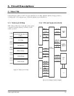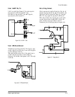
5-1-3 System Clock
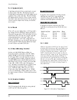
A high-speed clock and low-speed clock are used
for the system controller. The high-speed clock
39.3216 MHz is generated at external oscillator and
applied to the system controller. The CPU divides
the high-speed clock in two. They will be used for
bus clock and system clock source. The low-speed
clock is used for elapse time counter and refresh
rate counter.
5-1-4 Reset
When +5V power is higher than +4.5V (typically),
the voltage detector PST520C output goes 'High.'
The gate array generates CPU reset signal (Low) to
initialize the CPU. It causes the system controller
and peripheral device to be reset. When +5V
power drops below +4.5V, the voltage detector
PST520C output goes 'Low' and alerts main power
fail through CPU NMI (Non Maskable Interrupt)
pin and system controller PFAIL pin.
5-1-5 Bus & Memory Control
System controller BMC (Bus and Memory
Controller) interfaces directly with CPU, ROM,
SRAM, DRAM, and I/O device and generates
WAIT signal. BMC is divided into five zones by
decoding high-order address. The select signals
are SEL0 (ROM select), SEL1 (SRAM select), and
SEL2 (Gate Array select). It reads and writes data
when /RD, /WE0, /WE1, and /OE signal go
'Low'. Reading is activated always in Word-wide,
and writing is in Even byte when /WE0 goes
'Low', Odd byte when /WE1 goes 'Low' and
Word-wide when both signals go 'Low.' DRAM
access is controlled by /RAS0, /RAS1, and /CAS.
In order to access 8 Mbyte, /RAS0 is bank selected
by ASIC.
5-1-6 Scanner Control
IMAGE SENSOR
The CIS equipped with 300 dpi scanning density
and 2.5 ms for 1 line storage time.
IMAGE PROCESSOR
It supplies clock signal into CIS and performs
shading correction, AGC, edge emphasis,
correction, 64 gray levels, DMA, horizontal
reduction from 300 dpi A4 to 203 dpi A4.
SCAN MOTOR CONTROL
It supplies four phase strobes from system
controller to scan motor driver. Motor drives as
follows:
Motor Function
Strobe Pulse
Phase
Copy
400 pps
2-phase
Quick scan
600 pps
2-phase
Fine mode
600 pps
2-phase
Super fine mode
600 pps
1/2-phase
5-1-7 ASIC
ASIC is composed of LSU (Laser Scanning Unit)
interface, dpi conversion mode, smoothing mode,
external chip select decoder, DRAM bank select,
I/O port, print data line memory control, and
UART. In print mode, there are pass mode and
conversion mode. In pass mode, copy is made by
scanning at 300 dpi and printing at 300 dpi. In
conversion mode, it prints the received data after
406 dpi conversion through smoothing. UART is
also equipped to communicate with I-LIU chip in
9.6 k bps serial. LSU interface timing diagram is
provided below.
5-2
Samsung Electronics
Figure 5-3 LSU Interface Timing Diagram
Circuit Description
/HSYNC
/CHSYNC
SCLK
SDATA
/VDATA
/APCSH

