background image

SAMSUNG Proprietary-Contents may change without notice

Flow Chart of Troubleshooting

This Document can not be used without Samsung's authorization

7-15

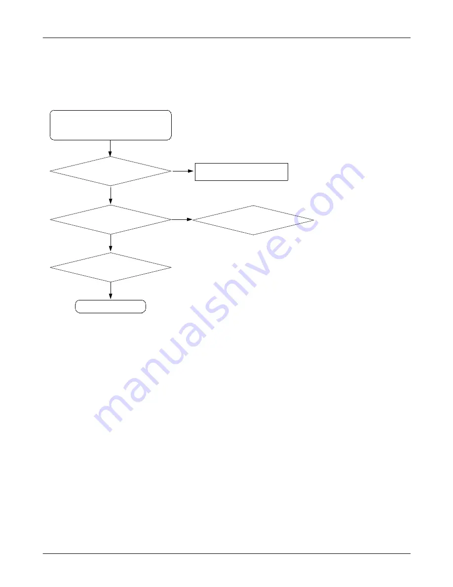
11. GSM Receiver

C104

>= -60dBm

Resolder U100

END

No

Yes

RX ON

RF input : CH center freq : +67.7kHz

Amp : -50dBm

Resolder F101

L103

>= -65dBm

Resolder U101

Yes

Yes

Yes

No

Summary of Contents for SGH-Z105

Page 1: ...SERVICE Manual UMTS TELEPHONE CONTENTS 1 Specification 2 Circuit Description 3 Exploded Views and Parts List 4 Electrical Parts List 5 Block Diagrams 6 PCB Diagrams 7 Flow Chart of Troubleshooting UMTS TELEPHONE ...

Page 2: ...nics Co Ltd April 2004 Printed in Korea Code No GH68 05056A BASIC ⓒ This Service Manual is a property of Samsung Electronics Co Ltd Any unauthorized use of Manual can be punished under applicable International and or domestic law ...

Page 3: ...805 1880 ARFCN range 1 124 0 124 975 1023 512 885 Tx Rx spacing 45MHz 45MHz 95MHz Mod Bit rate Bit Period 270 833kbps 3 692us 270 833kbps 3 692us 270 833kbps 3 692us Time Slot Period Frame Period 576 9us 4 615ms 576 9us 4 615ms 576 9us 4 615ms Modulation 0 3GMSK 0 3GMSK 0 3GMSK MS Power 33dBm 13dBm 33dBm 5dBm 30dBm 0dBm Power Class 5pcl 15pcl 5pcl 19pcl 0pcl 15pcl Sensitivity 102dBm 102dBm 100dBm ...

Page 4: ...2 dBm 7 29 2 dBm 8 27 2 dBm 9 25 2 dBm 10 23 2 dBm 11 21 2 dBm 12 19 2 dBm 13 17 2 dBm 14 15 2 dBm 15 13 2 dBm 16 11 3 dBm 17 9 3dBm 18 7 3 dBm 19 5 3 dBm TX Power control level DCS1800 0 30 3 dBm 1 28 3 dBm 2 26 3 dBm 3 24 3 dBm 4 22 3 dBm 5 20 3 dBm 6 18 3 dBm 7 16 3 dBm 8 14 3 dBm 9 12 4 dBm 10 10 4 dBm 11 8 4dBm 12 6 4 dBm 13 4 4 dBm 14 2 5 dBm 15 0 5 dBm 2 GSM TX power class ...

Page 5: ...r and the duplexer is highly recommended to provide constant load and source impedances respectively to those devices 6 UMTS PAM U202 This is a key component in the transmitter chain and must complement the RTR6200 IC precisely jointly they dominate the UMTS transmitter performance characteristics Parameters such as gain output power level ACLR harmonics Rx band noise and power supply current are ...

Page 6: ... front end design The UMTS input is configured differentially to optimize second order inter modulation and common mode rejection performance and implements MSM controlled gain adjustments to extend the receiver dynamic range 12 RTR6200 U101 The RTR6200 supports multi band multi mode phones with two receiver signal paths and three transmitter signal paths 1 Receiver paths EGSM 900 DCS 1800 2 Trans...

Page 7: ...t battery energy or excessive die temperature 1 2 Keypad Backlight The Keypad backlight driver output is at pin 17 KEYBD_DRV and is designed to drive parallel connected LEDs directly Its output current level is SBI programmable and meets the performance specified below Input parameters are not specified since they are internal 1 3 TCXO Controller and Buffers The PM6050 IC includes circuits for con...

Page 8: ...uipped 32 voices with different tones Since the device is capable of simultaneously generating up to synchronous with the play of the FM synthesizer various sampled voices can be used as sound effects Since the play data of YMU762MA3 are interpreted at anytime through data bus the length of the data playing period is not limited so the device can flexibly support application such as incoming call ...

Page 9: ... all by CPU Built in 32bit RISC CPU ARM7TDMI for control including H 245 and H 223 Built in 16bit DSP for audio CODEC Built in SD card I F Video input Rec601 YUV 4 2 2 8 bit I F Video output Rec601 YUV 4 2 2 8bit RGB 18bit Built in Picture In Picture Image Displaying Functions Built in On Screen Display OSD Functions Video CODEC 15fps for both encode and decode in QCIF size is possible Program on ...

Page 10: ...sung s authorization 3 1 1 Cellular phone Exploded View QMW03 QFU01 QCL06 QMO02 QSP01 QFL01 QMW02 QSC02 QCR01 QCW02 QCH02 QCA01 QCH05 QCR05 QCH06 QCH04 QCH01 QVO02 QFR01 QIF01 QKP01 QME01 QSH03 QMP01 QSC17 QAN01 QRF01 QRE01 QVO01 QCR01 QUA01 QUA05 KEY VOLUME CAMERA FOLDER UPPER SHIELD COVER MAIN WINDOW LCD IF COVER FRONT COVER WINDOW UPPER ...

Page 11: ...57A QCH04 CAMERA COVER GH71 02131A QCW02 CAMERA WINDOW GH72 09666A QCH02 CAMERA HOUSING GH72 12966A QCA01 CAMERA GH96 01500A QCH05 CAMERA SHAFT GH71 02656B QCR05 SCREW 6001 001478 QCH01 CAMERA HINGE DUMMY GH72 11107A QCH06 FRONT SIDE DUMMY GH75 04646A QVO02 KEY REJECT GH75 04237A QFR01 FRONT COVER GH75 04203A QIF01 IF COVER GH72 12149A QKP01 KEYPAD GH75 04205A QME01 METAL DOME GH59 01273A QSH03 SH...

Page 12: ...loded view and its Part list This Document can not be used without Samsung s authorization 3 3 3 Test Jig GH80 03305A 3 1 RF Test Cable GH39 00105A 3 2 Test Cable GH39 00210A 3 3 Serial Cable 3 4 Power Supply Cable 3 5 DATA CABLE GH39 00208A 3 6 TC GH44 00482A ...

Page 13: ...505 001131 Q701 0505 001332 U301 0505 001454 Q704 0505 001570 U304 0505 001570 U604 0505 001570 U708 0505 001570 U710 1001 001183 U533 1001 001183 U546 1001 001183 U703 1001 001225 U100 SEC Code Design LOC 1001 001231 U527 1001 001253 U547 1105 001489 U403 1109 001234 U401 1109 001243 U303 1201 001954 U102 1201 001984 U201 1201 001990 U202 1202 001036 U503 1203 002113 U606 1203 002965 U707 1203 00...

Page 14: ...12 2007 000148 R324 2007 000148 R327 2007 000148 R403 2007 000148 R603 2007 000148 R604 2007 000148 R612 2007 000148 R618 2007 000148 R709 2007 000148 R826 2007 000148 R836 SEC Code Design LOC 2007 000148 R837 2007 000148 U706 2007 000149 R335 2007 000152 R705 2007 000152 R707 2007 000152 R828 2007 000153 R317 2007 000153 R318 2007 000153 R401 2007 000153 R404 2007 000153 R414 2007 000153 R415 200...

Page 15: ...14 2007 000171 R606 2007 000171 R609 2007 000171 R622 2007 000171 R801 2007 000171 R802 2007 000171 R803 2007 000171 R804 2007 000171 R807 2007 000171 R809 2007 000171 R810 SEC Code Design LOC 2007 000171 R812 2007 000171 R813 2007 000171 R819 2007 000171 R820 2007 000171 R821 2007 000171 R822 2007 000171 R823 2007 000171 R825 2007 000171 R830 2007 000171 R831 2007 000171 R832 2007 000171 R833 200...

Page 16: ...23 2007 007138 R217 2007 007138 R219 2007 007142 R607 2007 007314 R201 2007 007314 R207 2007 007314 R209 2007 007314 R214 2007 007314 R325 2007 007318 R322 2007 007318 R506 SEC Code Design LOC 2007 007318 R507 2007 007334 R502 2007 007489 R839 2007 007491 R136 2007 007491 R208 2007 007528 R306 2007 007528 R307 2007 007538 R321 2007 007538 R611 2007 007698 R228 2007 007981 R614 2007 008117 R227 200...

Page 17: ...21 2203 000278 C622 2203 000278 C628 2203 000278 C632 2203 000278 C633 2203 000278 C636 2203 000278 C637 2203 000278 C638 2203 000278 C639 2203 000278 C710 2203 000311 C120 SEC Code Design LOC 2203 000330 C208 2203 000330 C211 2203 000330 C214 2203 000330 C245 2203 000386 C130 2203 000386 C137 2203 000386 C206 2203 000386 C255 2203 000386 C317 2203 000386 C319 2203 000386 C322 2203 000386 C325 220...

Page 18: ...09 2203 000812 C110 2203 000812 C112 2203 000812 C114 2203 000812 C116 2203 000812 C128 2203 000812 C133 2203 000812 C139 2203 000812 C160 2203 000812 C162 2203 000812 C166 SEC Code Design LOC 2203 000812 C249 2203 000812 C801 2203 000812 C802 2203 000812 C803 2203 000812 C804 2203 000812 C805 2203 000812 C807 2203 000812 C809 2203 000812 C813 2203 000812 C814 2203 000812 C815 2203 000812 C816 220...

Page 19: ...59 2203 003054 C867 2203 003054 C868 2203 003054 C869 2203 005054 C145 2203 005056 C117 2203 005061 C301 2203 005061 C302 2203 005061 C303 2203 005061 C304 2203 005061 C307 SEC Code Design LOC 2203 005061 C308 2203 005061 C309 2203 005061 C312 2203 005061 C313 2203 005061 C320 2203 005061 C324 2203 005061 C328 2203 005061 C336 2203 005061 C337 2203 005061 C339 2203 005061 C340 2203 005061 C343 220...

Page 20: ...63 2203 005482 C203 2203 005482 C222 2203 005482 C225 2203 005482 C234 2203 005482 C235 2203 005482 C239 2203 005482 C241 2203 005482 C243 2203 005482 C246 2203 005482 C254 SEC Code Design LOC 2203 005482 C259 2203 005482 C345 2203 005482 C353 2203 005482 C356 2203 005482 C412 2203 005482 C415 2203 005482 C507 2203 005482 C548 2203 005482 C609 2203 005482 C615 2203 005482 C616 2203 005482 C703 220...

Page 21: ... 2404 001086 C857 2404 001088 C643 2404 001105 C165 2404 001151 C321 2404 001239 C144 2404 001239 C341 2404 001239 C342 2404 001239 C515 2404 001239 C516 2404 001268 C614 SEC Code Design LOC 2404 001268 C709 2404 001281 C605 2404 001281 C606 2404 001281 C607 2404 001281 C619 2404 001281 C653 2703 001229 L606 2703 001229 L608 2703 001229 L609 2703 001259 L211 2703 001595 L118 2703 001724 L101 2703 ...

Page 22: ...5 2901 001286 F806 2901 001286 F807 2901 001286 F808 2901 001286 F809 2904 001417 F101 2904 001419 F102 2904 001438 F202 2904 001439 F201 2909 001202 F203 3301 001158 L601 3301 001158 L602 3301 001341 L113 3301 001341 L119 3301 001341 L301 3301 001341 L302 3301 001341 L303 3301 001341 L603 3301 001341 L604 3301 001341 L605 3705 001255 RFSW100 3709 001298 CN701 3710 001587 CN803 3710 002037 CN802 3...

Page 23: ...SAMSUNG Proprietary Contents may change without notice This Document can not be used without Samsung s authorization 5 SGH Z105 Block Diagrams 5 1 1 RF Solution Block Diagram ...

Page 24: ...SAMSUNG Proprietary Contents may change without notice Block Diagrams This Document can not be used without Samsung s authorization 5 2 2 Base Band Solution Block Diagram ...

Page 25: ...SAMSUNG Proprietary Contents may change without notice This Document can not be used without Samsung s authorization 6 SGH Z105 PCB Diagrams 6 1 1 Main PCB Top Diagram ...

Page 26: ...SAMSUNG Proprietary Contents may change without notice PCB Diagrams This Document can not be used without Samsung s authorization 6 2 2 Main PCB Bottom Diagram ...

Page 27: ...re than 3 4V Power On does not work Change the Battery END No Yes U601PIN27 PS_HOLD 2 8V Check the PMIC related to PS_HOLD No Yes Check the Clock at R610 32KHZ Resolder OSC610 No Yes C630 VDD_C 2 8V Check the PMIC No Yes C631 VDD_P 2 8V C629 VDD_A 2 6V Check the PMIC No Yes Check for the clock at C618 19 2MHz Check the clock generation circuit related to OSC202 No Yes Check the initial operation Y...

Page 28: ...100NF C608 C618 100PF TP601 10PF C637 10PF C632 VBATT MC 146 32 768KHz 20ppm OSC601 2 3 4 1 C610 10NF NC C620 3 1 2 DAN222TL D602 1UF C612 C624 NC BLM18PG300SN1D L602 10K 1 R607 C616 100NF 100NF C609 C615 100NF NC R625 VBATT_PMIC NC R601 C635 4 7UF 6 3V 6 3V 22UF C605 VBATT C627 1UF 6 3V C604 100NF PS_HOLD_N VREG_TCXO VREG_SYNT VREG_RFTX VDD_A VREG_BT VREG_RFRX TCXO_OUT SLEEP_XTAL_IN DLC_DETECT JI...

Page 29: ...ut notice Flow Chart of Troubleshooting This Document can not be used without Samsung s authorization 7 3 2 Initial TP601 PON_RESET H Initial Failure Check the PMIC END No Yes Is CN801 pin 13 28 LCD RESET OK Yes Yes No Check the LCD RESET Circuit ...

Page 30: ...zation Flow Chart of Troubleshooting 7 4 3 Sim Part CN701 pin 1 5 H Phone can t access SIM Card Check the SIM POWER Check the SIM Card END No Yes Yes Yes No Check the 32k OSC After Power ON Check USIM_CLK Signal on CN701 pin3 in a few second Yes No Replace PBA After SIM card insert CN701 pin 2 H USIM_RESET Yes ...

Page 31: ...is Document can not be used without Samsung s authorization 7 5 SIM 100NF C708 C707 NC VDD_LP ESDALC6V1W 5 ZD701 1 2 3 4 5 R707 20K 10PF C710 C706 NC G 9 10 G 1 1 2 2 3 3 4 4 5 5 6 6 7 G 8 G PC D6 A3 H3 0 S CN701 C713 68PF NDS332P Q701 D 3 G 1 S 2 USIM_RESET USIM_CLK USIM_DATA USIM_VCC_EN ...

Page 32: ...U510 pin7 32 2 8V Speaker does not work Check the Clock signal at Pin 1 of U510 13 5MHz Check the clock generation circuit related to U404 and U510 END No Yes No Resolder or replace U302 U510 pin 4 2 8V When U509 operate Resolder U509 Yes No U510 pin 15 Battery Volt Check the circuit related to AMP AMP signal Yes No Is Speaker working No Yes Change the Speaker Yes Yes ...

Page 33: ...RST 4 28 W R 18 15 SPVD D SPVSS 16 7 VDD 9 VREF VSS 8 C S 29 3 IRQ RD 10 11 HPOUT R IOVDD 32 LED 2 19 MTR 5 NC PLLC 6 17 SPOUT1 SPOUT2 20 EQ 1 12 13 EQ 2 EQ 3 14 33 G G 34 35 G G 36 HPOUT L MONO 1 CLKI D0 27 26 D1 25 D2 D3 24 23 D4 D5 22 21 D6 D7 U510 YMU762C QZE2 30 A0 2 8VDV C547 75PF 100NF C539 R515 C544 9PF 33K C536 1NF 22K R516 VBATT R511 51K FROMD 2 FROMD 3 FROMD 4 FROMD 5 FROMD 6 FROMD 7 AM...

Page 34: ...low Chart of Troubleshooting 7 8 5 Speaker Part Melody Check the connection from MIC Check the circuit from U302 to MIC Resolder MIC Resolder the R306 R307 R305 R308 C324 R851 R852 and C328 END No Yes Yes Yes Yes No Check the MIC No Replace the MIC Microphone does not work Yes U301 Pin6 GND No Resolder or Replace U528 ...

Page 35: ... authorization 7 9 Speaker C852 NC C327 15P F C332 9PF C331 9PF 7 EPJ5F 7 A1 DSP CN501 1 2 3 4 5 6 1 5K 1 R306 NC C851 3 G1 2 G2 5 1 S1 S2 4 FDG6301N U301 6 D1 D2 C320 100N F C319 15PF C318 9P F C325 15PF R307 1 5K 1 C326 47PF 100NF C328 C322 15PF 9PF C323 C321 33UF 6 3V R308 680 MICBIAS R305 680 C324 100NF MIC_P MIC_N MICBIAS_CONT ...

Page 36: ...sed without Samsung s authorization Flow Chart of Troubleshooting 7 10 6 Key Data Input When one of the keys is pushed is it displayed on LCD Check the Dome sheet Key Pad END No Yes Yes Check Initial Operation When one of the keys is pushed KEY_IO signal is OK Replace the PBA No Yes ...

Page 37: ... without Samsung s authorization 7 11 7 Receiver Part U302 pin Y7 2 8V Resolder or replace U302 END No Yes Yes Receiver does not work Is Receiver working Replace the Receiver No Yes No Resolder or replace C341 C342 Yes Check the soldering of the spaeaker wire No Modufy the speaker wire soldering Yes C341 C342 1 2V ...

Page 38: ...be used without Samsung s authorization Flow Chart of Troubleshooting 7 12 8 Back Light for Color Main LCD Is BACKLIGHT set AlwaysON in the Menu Set BACKLIGHT on AlwaysON END No Yes Yes Backlight does not work R327 2 8V Replace or Resolder R327 No Yes Yes Replace the LCD Module ...

Page 39: ...oubleshooting This Document can not be used without Samsung s authorization 7 13 9 Key Back Light Is BACKLIGHT set AlwaysON in the Menu Set BACKLIGHT on AlwaysON END No Yes Yes Key Backlight does not work CN804 pin 30 L No Resolder CN305 pin 30 or replace KeyPCB Module Yes ...

Page 40: ...n Flow Chart of Troubleshooting 7 14 10 Camera part Camera function does not work Yes No Connect the camera module Check the Camera connector on LCD module Yes R807 C415 2 8V No Replace or Resolder R807 C415 Yes R806 11 571MHz No Replace or Resolder R806 Yes Is there another problem END Replace the camera module Yes ...

Page 41: ...ce Flow Chart of Troubleshooting This Document can not be used without Samsung s authorization 7 15 11 GSM Receiver C104 60dBm Resolder U100 END No Yes RX ON RF input CH center freq 67 7kHz Amp 50dBm Resolder F101 L103 65dBm Resolder U101 Yes Yes Yes No ...

Page 42: ...ut Samsung s authorization Flow Chart of Troubleshooting 7 16 12 GSM Transmitter U102 Pin6 1V Resolder U102 TX ON 5Level Resolder OSC101 OSC101 pin5 2dBm U102 pin9 20dBm U101 pin3 30dBm Resolder U102 Resolder U101 OSC201 pin5 5m Yes No No No Yes Yes Yes Yes END Check U302 Resolder OSC201 Yes ...

Page 43: ...ce Flow Chart of Troubleshooting This Document can not be used without Samsung s authorization 7 17 13 DCS Receiver RX ON RF input CH center freq 67 7kHz Amp 50dBm Yes C106 60dBm Resolder U100 END No Yes Resolder F102 L107 65dBm Resolder U101 Yes Yes No ...

Page 44: ... Samsung s authorization Flow Chart of Troubleshooting 7 18 14 DCS Transmitter U102 Pin6 1V Resolder U102 TX ON 0Level Resolder OSC101 OSC101 pin5 2dBm U102 pin11 20dBm U101 pin3 30dBm Resolder U102 Resolder U101 OSC201 pin5 5m Yes No No No No Yes Yes Yes Yes END Check U302 Resolder OSC201 Yes ...

Page 45: ... without Samsung s authorization 7 19 15 WCDMA Receiver RX ON RF input CH center freq 67 7kHz Amp 50dBm Yes C208 60dBm Check Resolder U100 No Yes C214 65dBm C211 55dBm Yes Yes No Resolder F203 No Check Resolder U201 C230 60dBm Yes No Resolder F201 END Resolder U205 C250 20dBm Yes No Check Resolder OSC200 OSC202 Yes ...

Page 46: ...ow Chart of Troubleshooting 7 20 16 WCDMA Transmitter C250 20dBm Check Resolder OSC202 OSC201 TX ON PDM for 23dBm C212 5Bm C213 5dBm U202 pin4 20dBm Resolder F202 Check Resolder U202 U203 C208 20dBm Yes Yes Yes Yes Yes No No No No END Resolder MIS201 F203 No Check Resolder U101 Yes C101 20dBm Check Resolder U100 No Yes ...

Page 47: ... A 2 3 C 1 G 4 G R110 0 R109 0 L108 12nH NC L11 5 12nH L110 IN OUT 3 4 OUT 100 R130 R118 B7820 F101 G 25 G 1 L109 3 3n H 0 C129 100NF 10N F C153 C143 10NF 4 7PF C14 5 1 2nH L10 1 0 R11 3 R104 82 3 3K R142 C10 1 33P F R126 82 L119 C113 100N F VDDA 31 VDDA 34 VDDA 36 VDDA 14 VDDM ACZ1005M 121 T VDDA 42 VDDA VDDA 44 46 VDDA 15 VDDA VDDA 18 20 VDDA 23 VDDA 24 TX_MOD_CP 1 TX_QN 48 TX_QP 35 TX_VCO_IN 43...

Reviews: