
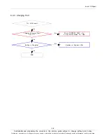
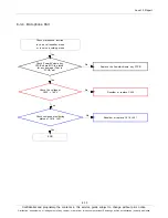
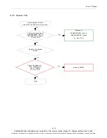
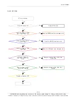
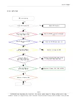
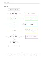
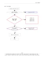
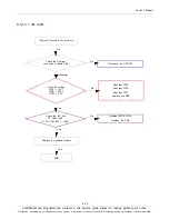
Level 3 Repair
Distribution, transmission, or infringement of any content or data from this document without Samsung’s written authorization is strictly prohibited.
Confidential and proprietary-the contents in this service guide subject to change without prior notice.
8-18
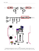
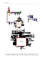
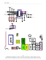
L226
C249
C240
L204
L207
L209
1
GND
P1
2
P2
4
3
P3
F200
1
1
2
2
ANT200
C242
C280
L227
L213
L208
L224
C241
L225
GND
1
3
GND
IN
4
OUT 2
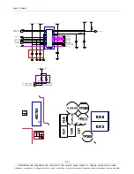
F203
LNA_ANT_5G
LNA_ANT_2G
C229
TP_WLAN_DAT201
C212
R212
C207
C211
C213
VDD_WIFI_1.8V
L
2
0
3
TP_WLAN_DAT203
TP_WLAN_DAT202
C203
N6
PWDET_2G
N7
W1_CNTL
N
8
L
V
L
D
O
_
V
IN
N9
GPIO11
VDD_WIFI_1.8V
N10
GPIO15
N
1
1
V
B
L
D
O
3
V
_
V
O
U
T
N
1
2
V
B
L
D
O
3
V
_
V
IN
N13
GPIO16
N
2
A
V
D
D
1
8
N
3
A
V
D
D
1
8
N4
XTAL_IN
N5
XTAL_OUT
M
3
A
V
D
D
1
8
M
4
A
V
D
D
1
8
M5
RBIAS
M
6
A
V
D
D
1
8
M7
PWDET_5G
M
8
L
V
L
D
O
_
V
O
U
T
GPIO12
M9
N
1
V
S
S
GPIO2
L13
L
2
A
V
D
D
1
8
M1
TX2_OUT
M10
GPIO14
M11
GPIO4
M12
GPIO1
M13
GPIO0
A
V
D
D
1
8
M
2
K
4
V
S
S
RES
K5
A
V
D
D
1
8
K
6
GPIO17
K7
K
8
V
D
D
1
2
K9
GPIO13
L
1
V
S
S
L12
GPIO3
J13
GPIO21
J2
V
S
S
V
S
S
J4
K1
RX2_IN
K10
GPIO6
K12
GPIO5
K13
GPIO7
K
2
V
S
S
H
2
A
V
D
D
1
8
H
4
V
S
S
H
6
V
S
S
H
7
V
S
S
H
8
V
S
S
J1
RX5_IN
J1
0
V
D
D
1
2
J12
GPIO8
G
4
V
D
D
3
0
G
6
V
S
S
G
7
V
S
S
V
S
S
G
8
H
1
V
S
S
H10
VIO
H12
GPIO22
H13
GPIO23
F
6
V
S
S
F
7
V
S
S
F
8
V
S
S
G1
TX5_OUT
G10
GPIO20
G12
SD_CLK
G13
SD_DAT3
G2
PA_PE_A
E2
RF_CNTL4_N
E4
RF_CNTL5_N
F1
PA_PE_G
F10
GPIO18
F12
SD_DAT1
F13
SD_DAT2
F2
RF_CNTL1_P
F4
RF_CNTL7_N
D
6
V
D
D
1
2
D7
RESETN
D8
GPIO10
D9
VIO
E1
RF_CNTL0_N
E10
GPIO19
E12
SD_CMD
E13
SD_DAT0
C2
RF_CNTL6_N
D1
RF_CNTL3_P
D
1
0
F
M
_
L
D
O
_
V
IN
D12
FM_AUDIO_OUT_R
D13
SLP_CLK_IN
D2
RF_CNTL2_N
D
4
V
S
S
D
5
V
S
S
B5
PDN
SER_WB
B6
B7
TDI
B8
TMS
B9
GPIO9
C
1
A
V
D
D
1
8
C12
FM_AUDIO_IN_R
C13
FM_AUDIO_OUT_L
B
1
A
V
S
S
B
1
0
A
V
D
D
1
8
B
1
1
F
M
_
L
D
O
_
V
O
U
T
B12
FM_AUDIO_IN_L
B
1
3
A
V
D
D
1
8
B
2
A
V
S
S
B
3
A
V
D
D
1
8
B
4
A
V
D
D
1
8
FM_ANT_TX
A13
A
3
A
V
D
D
1
8
A4
SER_DAT
A5
SER_CSN
A6
SER_CLK
A7
TDO
A8
TCK
A
9
A
V
D
D
1
8
1
N
C
N
C
2
A1
BRF_ANT
A
1
0
A
V
D
D
1
8
A
1
1
F
M
_
A
N
T
_
R
X
_
G
N
D
A12
FM_ANT_RX
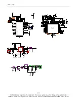
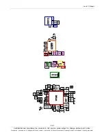
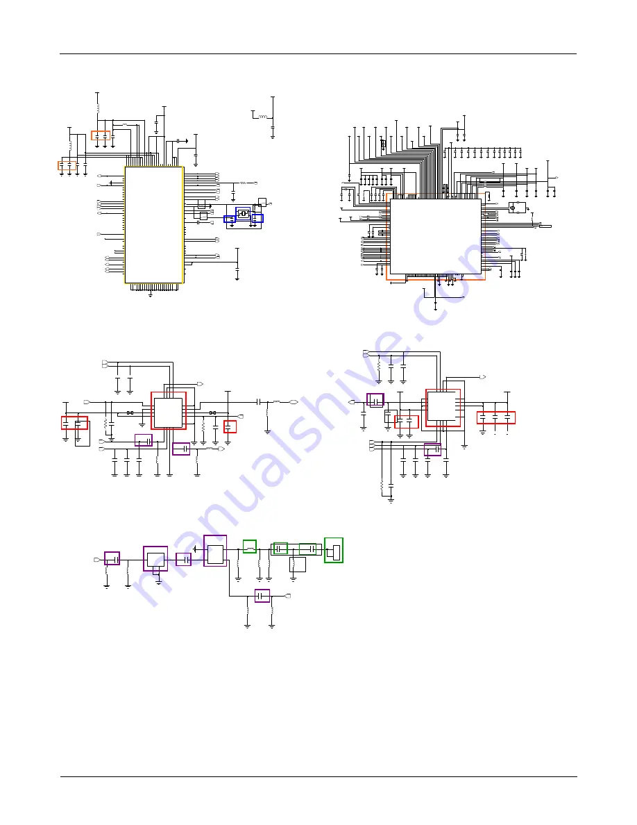
U202
TP_WLAN_CLK_EN
TP_WLAN_DAT200
TP_WLAN_WU_HOST
FM_ANT
C206
C210
TP_WLAN_BT_RESET
C205
VDD_WIFI_1.8V
C217
TP_WLAN_CMD
L200
FM_AUDIO_R
R209
R210
FM_AUDIO_L
VDD_WIFI_1.8V
C202
C235
VREG_1.8V
V_WIFI_3.3V
C204
TP_WLAN_PD
TP_HOST_WU_WLAN
VDD_WIFI_1.8V
L202
2.2nH
10
05
C209
L201
R206
CLK_26MHZ_WIFI
SW_WIFI_BT_RX
SW_BT_TX
SW_WIFI_5G_RX
LNA_EN_5
LNA_EN_2
CLK_32K_8787
PA_PE_A
PWDET_5G
TX_5
RX_5N
PWDET_2G
PA_PE_G
WLAN_PD
WLAN_BT_RESET
BRF
PCM_SYNC
WLAN_WU_HOST
PCM_CLK
PCM_RXD
PCM_TXD
HOST_WU_WLAN
WIFI_CLK_EN
WLAN_DAT0
WLAN_DAT1
WLAN_DAT2
WLAN_DAT3
WLAN_SD_CLK
WLAN_CMD
RX_2N
TX_2
C285
C230
R211
OSC201
2
4
3
1
R
2
1
9
C255
V_SYS
C266
C264
C254
V_SYS
R221
L215
L221
R202
L222
C274
L219
R222
R201
C268
L214
C258
C265
C272
C275
C267
C276
VCC
4
VCC
5
T
X
6
P
A
_E
N
7
G
N
D
8
R
X
9
LNA_EN
BT
12
GND
13
V
B
T
14
V
R
X
15
G
N
D
16
A
N
T
17
GND
2
GND
3
U208
1
VDET
10
VCC
11
LNA_ANT_2G
PWDET_2G
BRF
SW_BT_TX
SW_WIFI_BT_RX
PA_PE_G
LNA_EN_2
RX_2N
TX_2
C564
C519
C524
C526
V_CAM_IO_1.8V
V_ANALOG_3.0V
VREG_1.8V
C510
C520
VREG_LVS5_LVDS_1P8
C512
BAT500
C531
TP506
C513
VREG_L18_LVDS_1P2
C504
C549
VREG_1.2V
C501
TP511
C514
R500
VDD_DIG_1.8V
C509
TP501
TP515
SUBMIC_BIAS_1.65V
MIC_BIAS_1.65V
V_SYS
TP502
TP510
TP513
C547
V_VCTCXO_2.8V
TP504
V_PROXY_2.8V
VDD_DIG_1.8V
C539
TP516
V_SIM1_3.0V
C563
C508
V_GPS_1.8V
R503
R505
VREF1V2
V_2M_A2.8V
C540
C535
C548
C541
VCORE_MAIN_1.2V
C530
V_DIGRF_1.8V
VREG_1.2V
C584
C503
C538
C560
C529
C561
TP505
C502
VREG_1.8V
C525
VREG_1.8V
C537
TP500
C507
C554
V_SYS
OSC500
2
1
C546
TP509
EAR_MIC_BIAS_2.6V
C528
V_WIFI_3.3V
TP514
C550
C521
C566
C511
L503
C522
L501
L500
C527
C
5
3
4
VREG_L16_LVDS_3P3
TH500
V_SD_3.0V
C518
V_USB_3.1V
C500
C544
C536
C523
1005
C579
C562
C506
C505
VREF1V2
T
2
V
L
D
O
1
2
T3
DVC2
T
4
V
L
D
O
1
0
T
5
V
L
D
O
9
T
6
V
L
D
O
8
T
7
V
L
D
O
7
T
8
V
L
D
O
6
T
9
P
G
N
D
_
B
U
C
K
1
R
7
V
S
S
R8
SLEEPN
R
9
P
G
N
D
_
B
U
C
K
1
T
1
N
C
-T
1
T
1
0
V
X
_
B
U
C
K
1
T
1
1
V
IN
_
B
U
C
K
1
T
1
2
V
X
_
B
U
C
K
2
T
1
3
N
C
-T
1
3
R
1
1
V
IN
_
B
U
C
K
1
R
1
2
V
IN
_
B
U
C
K
2
R
1
3
P
G
N
D
_
B
U
C
K
2
R
2
V
L
D
O
1
3
R
3
V
B
U
C
K
3
R
4
V
S
S
R
5
V
L
D
O
1
1
R6
DVC1
P
4
V
S
S
P
5
V
IN
6
P
6
V
IN
5
P
7
V
IN
4
P
8
V
S
S
P
9
V
S
S
R
1
V
X
_
B
U
C
K
3
R
1
0
V
X
_
B
U
C
K
1
N
3
V
S
S
P
1
V
IN
_
B
U
C
K
3
P
1
0
V
S
S
P
1
1
V
IN
2
P
1
2
V
B
U
C
K
2
P13
PMODE
P
2
P
G
N
D
_
B
U
C
K
3
P
3
V
B
U
C
K
4
M
6
V
S
S
M
7
V
S
S
M8
RESET_OUTN
M9
EXTONN
N
1
V
IN
_
B
U
C
K
4
N
1
2
V
B
U
C
K
1
N13
ONKEYN
N
2
V
S
S
L8
PMIC_INTN
L9
VBAT_SNS
M
1
V
X
_
B
U
C
K
4
M
1
2
V
L
D
O
5
M13
VSC
M
2
P
G
N
D
_
B
U
C
K
4
M
3
V
S
S
M5
GPIO2
L11
VCHG_GOOD
L
1
2
V
L
D
O
4
L13
GPADC5
L
2
V
L
D
O
1
4
L
3
V
IN
7
L5
CLK32K_2
L
6
V
S
S
L
7
V
D
D
IO
1
K
2
V
L
D
O
1
6
K
3
V
IN
8
K5
PWM
K
6
V
S
S
K
7
V
S
S
K8
GPIO0
K9
CLK32K_1
L
1
V
L
D
O
1
5
J6
CLK32K_3
J
7
V
S
Y
S
J
8
V
S
S
J9
GPIO3|HDET
K
1
V
L
D
O
1
7
K11
GPADC1
K
1
2
V
L
D
O
3
K
1
3
V
L
D
O
2
H
9
A
G
N
D
J
1
V
D
D
_
S
P
K
N
J11
GPADC4
J
1
2
V
L
D
O
1
J
1
3
V
IN
1
J
2
V
D
D
A
_
S
P
K
J
3
V
D
D
A
_
S
P
K
_
D
E
J5
VAON
H12
GPADC0
H13
GPADC3
H
2
G
N
D
S
P
K
H3
GPIO1
H
5
V
S
S
H
6
V
IN
3
H
7
V
D
D
IO
3
H
8
V
S
S
G
3
V
S
S
G
5
V
L
D
O
1
8
G
6
V
L
D
O
1
9
G7
VINREF
G8
VREF1V2
G
9
G
N
D
R
E
F
H1
SPKN
H
1
1
V
B
U
C
K
5
F7
MICVDD12/AMICB1
F8
AMICPEXT
F
9
G
N
D
A
N
A
G1
SPKP
G11
REFNADC
G12
GPADC2
G
1
3
V
IN
_
B
U
C
K
5
G
2
V
S
S
E9
REFCLK
F
1
V
D
D
_
S
P
K
P
F11
REFPADC
F
1
3
V
X
_
B
U
C
K
5
F
2
P
W
M
_
G
N
D
F
3
V
S
S
F5
MICDAT12/AMICP1
F6
MICCLK12/AMICN1
E12
ANAPOS
E
1
3
P
G
N
D
_
B
U
C
K
5
E2
XTAL2
E3
XTAL1
E5
AUX2P
E6
AUX2N
E7
AMICNEXT
E8
ANANEG
D1
AUX1P
D11
EARN
D12
AMICBEXT
D
1
3
G
N
D
E
A
R
D2
AUX1N
D3
MICDAT34/AMICP2
E
1
V
D
D
1
2
C
L
E
A
N
E11
EARP
C
1
1
V
S
S
C12
REFDAC
C
1
3
V
D
D
1
8
P
C
2
V
D
D
IO
2
C
3
V
S
S
C
4
V
D
D
C
O
D
E
C
C5
MICCLK34/AMICN2
C9
REFCCURR
B3
SDI1
B4
FSYN1
B5
MICVDD34/AMICB2
B6
SDO1
B8
CTPCPLV
B
9
G
N
D
C
P
C1
I2C_SDA
C10
HP1
A8
CTNCPLV
A9
BCLK2
B1
I2C_SCL
B10
HP2
B
1
1
V
D
D
1
8
N
B
1
2
S
N
S
G
N
D
B
1
3
V
D
D
0
6
P
B2
PDM_DATA
A12
CTNCPHV
A
1
3
N
C
-A
1
3
A2
PDM_CLK
A3
CODEC_INTN
A4
BCLK1
A5
SDI2
A6
SDO2
A7
FSYN2
N
C
1
N
C
2
A
1
N
C
-A
1
A
1
0
V
D
D
0
6
N
A11
CTPCPHV
V_MMC_3.0V
PM500
TP512
L502
TP503
2M_CAM_CORE_1.8V
V_MOTOR_3.3V
C532
C517
TP508
VLED_IC_1.9V
V_SYS
C580
1005
C
5
3
3
L504
Audio_R_3.5
PCM_RXD
SUB_MIC_N
SUB_MIC_P
SPK_ROUT_N
SPK_ROUT_P
PMIC_32KHZ_OUT3
CLK_32K_8787
CLK_32KHZ_AGPS
RF_TEMP
PDM_CLK
PDM_DATA
LCD_SELECT
Audio_L_3.5
TSP_VENDOR2
PMIC_GPIO2
PCM_TXD
PMIC_32KHZ_OUT1
GND_HS_SENSE
ANAPOS
V_CORE_SNS
VLT_LVL_SEL1
VCXO_EN
VLT_LVL_SEL2
PCM_SYNC
PCM_CLK
TSP_VENDOR1
PMIC_INTN
VBAT_SENSE
PMIC_RST_OUT
ANAPOS
PMIC_32KHZ_OUT3
EAR_ADC_3.5
L_DET
VF
CODEC_INTN
HIFI_BITCLK
CI2C_SCL
HIFI_SDATA_OUT
HIFI_SYNC
HIFI_SDATA_IN
CI2C_SDA
TA_EN
MAIN_MIC_P
MAIN_MIC_N
EAR_MIC_P
EAR_MIC_N
RCV_N
RCV_P
JIG_ON_N
ON_SW
V_CORE_SNS
C281
R
2
1
8
C262
C244
C257
V_SYS
V_SYS
R216
C282
C261
C256
C260
22pF
R217
C252
C250
C259
2
RX
3
GND
4
VCC
5
V
D
E
T
6
P
A
_
E
N
7
G
N
D
8
T
X
9
GND
10
VCC
11
VCC
12
GND
1
3
A
N
T
1
4
G
N
D
1
5
V
R
X
1
6
L
N
A
_
E
N
1
7
GND
U207
1
GND
C253
C283
C251
C263
PA_PE_A
LNA_ANT_5G
PWDET_5G
LNA_EN_5
SW_WIFI_5G_RX
RX_5N
TX_5