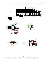
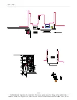

Level 3 Repair
Distribution, transmission, or infringement of any content or data from this document without Samsung’s written authorization is strictly prohibited.
Confidential and proprietary-the contents in this service guide subject to change without prior notice.
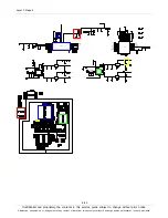
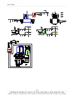
8-46
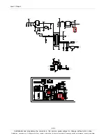
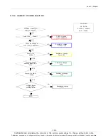
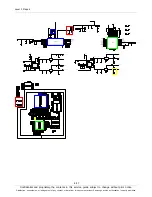
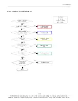
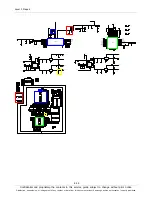
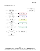
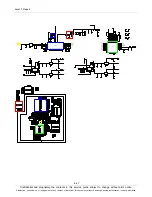
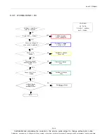
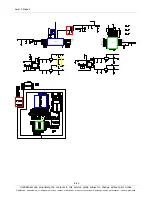
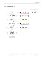
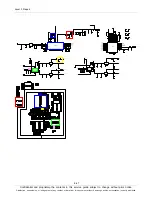
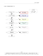
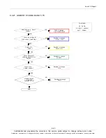
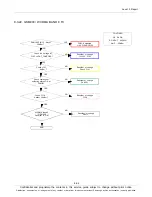
8-3-19. WCDMA BAND 1 TX
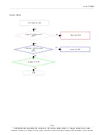
CONTINUO
US RX ON
RF INPUT : 4408CH
AMP : -50dBm
PAM100 PIN 15 : About
30dBm ?
Check the Voltage at
C105 =VOUT_CHARGER ?
Check component
soldering status OK at
PAM101
CHECK soldered
L104,C108,RFS100
Resolder or change
PAM
100, C105
Resolder or change
PAM101
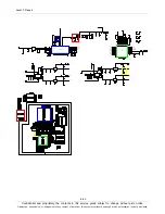
Check L127
≥
-
30
dBm ?
Resolder or change
Check C129
WCDMA Band5
/ GSM 850
Receiver is O.K?
Resolder or change
U401-1
END
YES
NO
NO
YES
NO
YES
NO
YES
NO
Check C174
:
Aabout 30dBm ?
Resolder or change
C139
NO
YES