background image

Alignment and Adjustments

5-8

Samsung Electronics

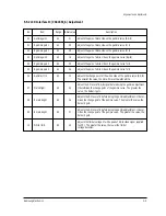
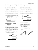
5-6-1 LCD Control Board PLL Adjustment 

1.  Input a color bar signal.

2.  Connect CNL06,RPD to an oscilloscope, and

check the waveforms.
(1 V/div, 20 u sec/div)

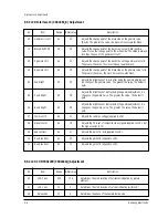
5-6-2 Matrix IC (TDA4780) Sub Tint Adjustment 

1.  Input a color bar signal.

2.  Connect CNL07 (B output) to an oscilloscope,

and check the waveform.
(0.5 V/div, 20 u sec/div)

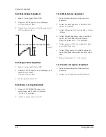
5-6-3 Matrix R Output Signal Amplitude 

Adjustment (Red Drive)

1.  Input a 10-step signal (Color OFF).

2.  Connect CNL07 (R output) to an oscilloscope,

and check the waveform.      
(0.5 V/div, 10 u sec/div)

3.  Adjust the red drive so that the signal ampli-

tude becomes 0.7Vp-p.

4.  Adjust the Sub-brightness of TDA4780 so that

the waveform (without sync) is seen as shown
in the figure below.

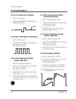
5-6-4 Matrix G Output Signal Amplitude 

Adjustment (Green Drive)

1.  Input a 10-step signal (Color OFF).

2.  Connect CNL07 (G output) to an oscilloscope,

and check the waveform.    
(0.5 V/div, 10 u sec/div)

3. Adjust the green drive so that the signal

amplitude becomes 0.7Vp-p.

5-6- 5 Matrix B Output Signal Amplitude 

Adjustment (Blue Drive)

1.  Input a 10-step signal (Color OFF).

2.  Connect CNL07 (B output) to an oscilloscope,

and check the waveform. 

(0.5 V/div, 10 u sec/div)

3.  Adjust the blue drive so that the signal ampli-

tude becomes 0.7Vp-p.

5-6-6 Main Brightness Adjustment

1.  Input a 10-step signal (Color OFF). 

2.  Connect LCD CNL08(R1) input to an oscillo-

scope, and check the waveform.
(2 V/div, 10 u sec/div)

3.  Adjust the main brightness so that the Ref

pulse is positioned on the center of signal. 

Note : The change point (on gamma curve) is  

determined by Ref.

RPD

DC2.8V

5-6 Circuit Adjustments

REF Pulse 

Summary of Contents for SP43J6HDX/XEN

Page 1: ...EN SP43J6HDX VWT COLOR TELEVISION RECEIVER CONTENTS Precautions Reference Information Specifications Disassembly and Reassembly Alignment and Adjustments Troubleshooting Exploded View and Parts List Electric Parts List Block Diagram Schematic Diagrams 1 2 3 4 5 6 7 8 9 10 ...

Page 2: ...ELECTRONICS Samsung Electronics Co Ltd MAY 2000 Printed in Korea 3M51A 4308 ...

Page 3: ...ts metal cabinets screwheads and control shafts The current measured should not exceed 0 5 milliamp Reverse the power plug prongs in the AC outlet and repeat the test Fig 1 1 AC Leakage Test 6 Antenna Cold Check With the unit s AC plug disconnected from the AC source connect an electrical jumper across the two AC prongs Connect one lead of the ohmmeter to an AC prong Connect the other lead to the ...

Page 4: ...t appear to have overheated or that are otherwise damaged should be replaced with parts that meet the original specifications Always determine the cause of damage or overheat ing and correct any potential hazards 15 Observe the original lead dress especially near the following areas Antenna wiring sharp edges and especially the AC and high voltage power supplies Always inspect for pinched out of p...

Page 5: ...t terminals and earphone jacks 6 Insulation Checking Procedure Disconnect the power cord from the AC source and turn the power switch ON Connect an insulation resistance meter 500V to the blades of the AC plug The insulation resistance between each blade of the AC plug and accessible conductive parts see above should be greater than 1 megohm 7 Never defeat any of the B voltage interlocks Do not ap...

Page 6: ...trical charges that damage ESDs 5 Use only a grounded tip soldering iron when soldering or unsoldering ESDs 6 Use only an anti static solder removal device Many solder removal devices are not rated as anti static these can accumulate sufficient electrical charge to damage ESDs 7 Do not remove a replacement ESD from its protective package until you are ready to install it Most replacement ESDs are ...

Page 7: ...rtz Hour Inches Per Second Kilowatt hour Kilogram Kilohertz Kilohm Kilometer Kilometer Per Hour Kilovolt Kilovolt ampere Kilowatt Liter Megahertz MV MW MΩ m µA µF µH µm µs µW mA mg mH mI mm ms mV nF Ω pF Ib rpm rps s V VA W Wh Megavolt Megawatt Megohm Meter Microampere Microfarad Microhenry Micrometer Microsecond Microwatt Milliampere Milligram Millihenry Milliliter Millimeter Millisecond Millivol...

Page 8: ...e Ground Green Y High High Frequency High Fidelity Inductance Capacitance Integrated Circuit Intermediate Frequency I O L L LED LF MOSFET MTS NAB NEC NTSC OSD PCB PLL PWM QIF R RC RF R Y SAP SAW SIF SMPS S N SW TP TTL TV UHF UL UV VCD VCO VCXO VHF VIF VR VTR VTVM TR Input output Left Low Light Emitting Diode Low Frequency Metal Oxide Semiconductor Field Effect Tr Multi channel Television Sound Nat...

Page 9: ...FAN LEVER S W THERMO S W DETECT LED CONTROL LAMP ON OFF 7 5 VIDEO S W VIDEO S W OP AMP SOUND PROCESSOR DOLBY PRO LOGIC OP AMP ANALOG MULTIPLEXER 8 BIT MICRO CONTROLLER EEPROM 2K 8 PROGRAMMABLE ROM MEGATEXT DRAM 1M 4BIT MULTIVIBRATOR CMOS LOGIC RGB CONTROL DAC RGB DRIVER SAMPLE HOLD DRIVER TIMING GENERATOR COMPONENT INTERFACE PROCESSOR VIDEO PROCESSOR POWER ON RESET GENERATOR DISPLAY PROCESSOR VIDE...

Page 10: ...2 4 Samsung Electronics MEMO ...

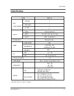
Page 11: ...able Main Voltage 230V Input Range 220 240V 50Hz 1 43 16 9 p Si Active matrix TFT 100 VHF 2 12 UHF 21 69 Cable S1 S41 1 RCA Input 1 S Video input Headphone Audio Output EXT1 full RGB Scart AV LINK EXT2 Scart Output Selectable EXT3 Decoder Output Selectable Dolby Prologic Signal Output RCA Jack Specifications are subject to change MODEL ANTENNA INPUT NUMBER OF CHANNELS TUNING RANGE SOUND OUTPUT SOC...

Page 12: ...3 2 Samsung Electronics MEMO ...

Page 13: ...assembly 4 1 Back Cover Removal 1 After removing the screws pull the bottom and side holder part of the cabinet back wards 2 Loosen the screws and remove the supporter 4 Loosen the screws Remove the front mask 3 After loosening the screws remove the lens cover and fan duct ...

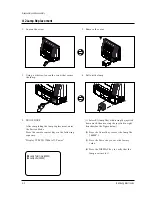
Page 14: ...ent enter the Service Mode Press the remote control Keys in the following sequence Display P STD Mute Power 1 Select 01 lamp life with using the joystick downward then moving the joystick to right directior See the figure below 2 Press the Cancel key to reset the lamp life 00000 3 Press the Power key to save the factory value 4 Press the DISPLAY key to verify that the lamp use time is ø 00 Lamp To...

Page 15: ...ectronics 4 3 4 2 1 Lamp Bulb only Replacement 1 Loosen the screw 3 After loosening bracket remove the lamp holder and wires 2 Remove the lamp bracket after loosen two screws from the lamp assembly 4 After loosening screws remove the bulb ...

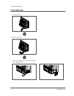
Page 16: ...Disassembly and Reassembly 4 4 Samsung Electronics 4 3 Air Filter Check 2 Remove the cover 3 After removing the holder and filter from the cover clean the filter 1 Loosen the screw ...

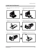
Page 17: ...abinet backwards 3 Remove the dust cover and disjoint the FPC connector 5 Pull out the LCD panel 2 Loosen the 2 screws and remove the airfilter at the right side then pull out the optical engine 4 Loosen the 2 screws and be careful to do not bend the LCD panel bracket 6 Be careful there is no finger print or dust on the LCD panel ...

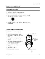
Page 18: ...ocus Adjustment for projection Lens 1 Loosen the 4 screws that secure the optical assembly 2 After setting the optical assembly on the front cabinet secure the unit temporarily using the two screws 3 After applying the liquid crystal panel signal input a lion head pattern from a pattern generator 4 Move the focus adjustment screws right and left until the liquid crystal picture element is clearly ...

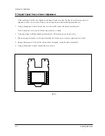
Page 19: ...the two screws that secure the liquid crystal panel Note Loosen the screws just until the panel can move easily 2 Using two fingers lift the liquid crystal upward The screen moves downward 3 When moving the liquid crystal panel towards the left the screen moves right and vice versa 5 Repeat adjustments 2 4 until the screen center is aligned vertically and horizontally 6 Using a hexagonal wrench re...

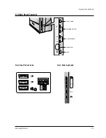
Page 20: ...Alignment and Adjustments Samsung Electronics 5 3 5 4 Side Panel Controls 5 4 1 Rear Panel Jacks 5 4 2 Side input jack ACCESS TO MENU PROGRAMME SELECTION VOLUME ADJUSTMENT LED INDICATORS POWER ...

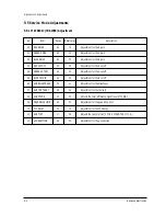
Page 21: ... DELAY SUB TINT γ CORRECTION 63 63 63 63 63 63 20 20 20 63 15 17 63 19 14 23 32 32 32 11 20 00 53 10 09 00 Adjustment for the R gain Adjustment for the G gain Adjustment for the B gain Adjustment for the R cutoff Adjustment for the G cutoff Adjustment for the B cutoff Adjustment for the brightness Adjustment for the contrast Adjusts the color difference signal level of YUVIN 1 Adjustment for the p...

Page 22: ...in of white side on the gamma curve for R Adjusts the gain of white side on the gamma curve for R Adjusts the change point of the white side on the gamma curve R G B The smaller the value the more it moves towards white Adjust the DC level of R G B signal before doing the gamma adjustment It determines the change point of the gamma curve The greater the value the darker it gets Adjusts the DC leve...

Page 23: ... black side on the gamma curve for B The greater the value the more it moves towards black Adjusts the brightness of R G B after doing the gamma adjustment No change of the gamma curve The greater the value the darker it gets Adjusts the brightness of R after doing the gamma adjustment No change on the gamma curve The greater the value the darker it gets Adjusts the brightness of B after doing the...

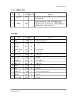
Page 24: ...t must be done after lamp replacement 5 5 5 Lamp s Total Hours 5 5 6 Option No Item Range Initial value Description 00 01 02 03 04 05 06 07 08 09 10 11 12 13 Epg Av_link Palplus 27Mhz external 16 9 wide Dolby prologic 3d sound S audio mute Blue screen UHF only Vga Atm one run Size key Vert peaking on off on off on off on off on off on off on off on off on off on off on off on off on off on off off...

Page 25: ...n as shown in the figure below 5 6 4 Matrix G Output Signal Amplitude Adjustment Green Drive 1 Input a 10 step signal Color OFF 2 Connect CNL07 G output to an oscilloscope and check the waveform 0 5 V div 10 u sec div 3 Adjust the green drive so that the signal amplitude becomes 0 7Vp p 5 6 5 Matrix B Output Signal Amplitude Adjustment Blue Drive 1 Input a 10 step signal Color OFF 2 Connect CNL07 ...

Page 26: ... to LCD R1 input 1 V div 10 u sec div 3 Reverse the CH2 signal and add CH1 and CH2 in ADD mode 4 Adjust R sub contrast and R sub brightness waveforms as shown below 5 6 9 B Sub brightness B Contrast Adjustments 1 Input a 5 step signal Color OFF 2 Connect CH1 to LCD G1 input and CH2 to LCD B1 input 1 V div 10 u sec div 3 Reverse the CH2 signal and add CH1 and CH2 in ADD mode 4 Adjust B sub contrast...

Page 27: ...orm 1 V div 10 u sec div 2 Set the common control to 6 8V 5 6 14 White Balance Adjustment 1 Input a lion head pattern from a pattern generator 2 Adjust the sub brightness so that the white cannot be saturated 3 Adjust R B contrast for the high light of white balance 4 Adjust R B sub brightness when the middle tone is not black and white but colored Repeat adjustments 3 4 for optimum 5 Adjust gamma...

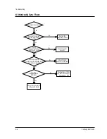
Page 28: ... Clean the air vent cover in the rear of the TV Turn the TV back on after 1 hour see below Temperature The lamp needs to be replaced or OFF ON Blinking Temperature Wen the inside temperature of the TV becomes too high the TV set is automatically turned off You will observe the following 1 TEMP LED is blinking for about 5 6 seconds 2 The picture is turned to blue screen and TEMPERATURE character bl...

Page 29: ...emote control keys in the following sequence Display Picture Standard Mute Power 2 Use the Channel UP DOWN keys to move within the Service Mode 3 Use the Vol key and Vol key to change data 1 Press the Vol key to increase data 2 Press the Vol key to decrease data 4 Use the Power key to exit and store data in memory ...

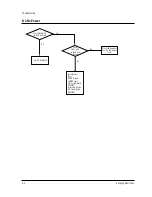
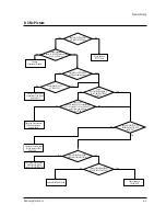
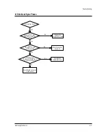
Page 30: ... Yes Check Stand by 5V on the Main Board See 6 5 No Standy Check Replace Tuner MICOM Module AUDIO Module A V Terminal Board TDA6920 Progressive Module LCD Control Board TDA4780 Check SDA1 SCL1 on the Micom Module Check LED Operation See 5 7 LED Display Check No ...

Page 31: ...ce the IC No Check ICL404 TDA4780 6 B Y 7 R Y 8 Y 27 SDA 28 SCL Yes Yes No Check CL129 130 131 and AC2 5P connector for 6 7 8 Check AC1 12P and SDA SCL output of micom module for 27 28 Check the circuitry near ICL404 and replace micom module No Check the circuitry near ICL404 replace IC201 TDA4780 Check ICL404 TDA4780 20 B OUT 22 G OUT 24 R OUT Check ICL204 CXA1853Q 9 R in 10 G in 11 B in No No Ch...

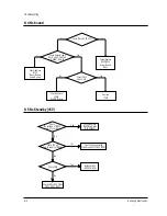
Page 32: ...dule MAIN L SUR CENTER S RESET QSS IN Check IC604 9 14 15 Check Replace IC604 MICOM Module No Replace IC601 Yes 6 5 No Standby 5V Yes No No No Yes Yes Check the voltage of IC808 pin 5 over 6V Check Replace IC808 Regulator IC SI 3050C Check the AC power supply of D826 Check the associated circuitry parts of T802 IC801 Check F801 Replace F801 AC250V 6 3A Check L801 L802 C801 C802 V801 R801 ...

Page 33: ...ns 6 7 Lamp Does Not Work Yes No No Yes Standby Temp LED Picture LED Lamp LED flicker at the same time Or check the lamp time 6000 hrs Check Replace Lamp Check the DC voltage of BALLAST about 300V Check the voltage of AB1 connector pin1 on the Main Board over 3 5V Check F801 on the Power Board D803 and surrounding circuitry Check the voltage of IC904 SAA1300 pin 6 over 3 5V on the Main Board Check...

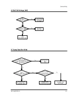
Page 34: ...e module Replace the progressive module Check Connector Assy AC1 Check the input of 2H sync to ICL301 CXD2443Q Pin 13 on the LCD Control Board Check ICL402 74HC123 Pin13 FI302 Check the voltage of CNL06 RPD 2 8V Check voltage of TL301 so that the voltage of CNL06 RPD is 2 8V Check the output of 2H Sync HREF to LCD Control Board Check the connector to LCD panel CNL04 ...

Page 35: ...l Sync Flows Check the output of V Sync HREF from progressive module Replace the progressive module Check Connector Assy AC1 Check the input of V Sync to ICL301 Pin 14 on LCD Control Board Check ICL402 74HC123 Pin 5 Check the input of V Sync to LCD Control Board Check CNL04 connector to LCD panel ...

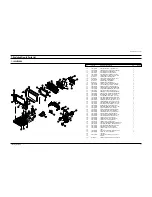
Page 36: ...3J6 AL6063 BLK 2 2 12 AA61 00406B BRACKET SCREEN TOP 43J6 AL6063 BLK E 2 2 13 AA67 00051A SCREEN LENTICULAR 43W PMMA T2 1 9 1 2 14 AA67 00050A SCREEN FRESNEL 43W PMMA T2 0 973 1 3 1 AA61 00183B BRACKET MIRROR LCD 43J6 SECC 1 T1 6 BL 1 3 2 AA61 00360B BRACKET SIDE LCD 43J6 SECC 1 T1 0 BLK 2 3 3 AA67 00057A MIRROR FRONT 43W GLASS T3 0 FSM 1 3 4 AA61 00184B BRACKET MIRROR TOP 43J6 SECC 1 T1 6 BL 1 3 ...

Page 37: ...7P TANTUS LCD HIPS HB GRAY ASSY ACCESSORY I B AA68 00802AMANUAL USERS M51A W P100 G 56P B5 1 GER GER I B AA68 00835AMANUAL USERS M51A W P100 G 56P B5 1 ITALY 8 2 SP43J6HDX VWT SP43J6HDX XEN and SP43J6HDX VWT Dissimilar Parts Loc No Code No Description Specification Remark Loc No Code No Description Specification Remark ASSY PCB MAIN OPT AA94 01910P ASSY PCB MAIN OPT SP43J6HDX VWT M51A LITHUA NIA V...

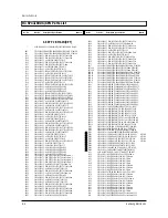
Page 38: ...HR TP 10x20mm 5m C870 2305 000665 C FILM MPEF 100nF 5 63V TP 7 5x4 0x5 0m C901 2305 000665 C FILM MPEF 100nF 5 63V TP 7 5x4 0x5 0m C902 2401 000914 C AL 22uF 20 16V GP TP 5x11 5 C903 2301 000383 C FILM PEF 10nF 5 50V TP 6x7x3 2mm 5mm C904 2401 002300 C AL 47uF 20 50V GP TP 6 3x11 5 C905 2301 000356 C FILM PEF 47nF 5 50V TP 7 5x4 0x6 5 5m C907 2305 000411 C FILM MPEF 470nF 5 50V TP 7 3x4 8x5 5m C90...

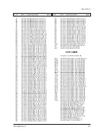
Page 39: ...2MM R901 2001 000577 R CARBON 2KOHM 5 1 8W AA TP 1 8X3 2MM R902 2001 000577 R CARBON 2KOHM 5 1 8W AA TP 1 8X3 2MM R903 2001 000613 R CARBON 3 9KOHM 5 1 8W AA TP 1 8X3 2M R904 2001 000290 R CARBON 10KOHM 5 1 8W AA TP 1 8X3 2MM R905 2001 000734 R CARBON 4 7KOHM 5 1 8W AA TP 1 8X3 2M R906 2001 000723 R CARBON 4 3KOHM 5 1 8W AA TP 1 8X3 2M R907 2001 000273 R CARBON 100KOHM 5 1 8W AA TP 1 8X3 2M R908 2...

Page 40: ...CABINET MAIN AA91 00291AASSY CABINET MAIN VO PS BLK 43J6 BG CM 6002 000522 SCREW TAPPING TH 2 M4 L15 ZPC BLK SWR HM CM 6002 000522 SCREW TAPPING TH 2 M4 L15 ZPC BLK SWR SPC CM 6002 000522 SCREW TAPPING TH 2 M4 L15 ZPC BLK SWR SPT CM 6003 001023 SCREW TAPTITE RWH B M3 L10 ZPC YEL SW SPW CM 6002 000522 SCREW TAPPING TH 2 M4 L15 ZPC BLK SWR AA60 00033ASPACER LENS P U FOAM V0 16 BLK 50J6 AA61 00165B B...

Page 41: ...203 000170 C CERAMIC CHIP 1 8nF 10 50V X7R TP 2012 CB1 2401 000365 C AL 100uF 20 50V WT TP 10x12 5mm CD601 2203 000260 C CERAMIC CHIP 10nF 10 50V X7R TP 2012 CD602 2203 000142 C CERAMIC CHIP 1 5nF 10 50V X7R TP 2012 CD603 2401 000962 C AL 22uF 20 50V GP TP 5x11 5 CD604 2203 000595 C CERAMIC CHIP 0 22nF 5 50V NP0 TP 2012 CD605 2203 000938 C CERAMIC CHIP 0 47nF 5 50V NP0 TP 2012 CD606 2401 000962 C ...

Page 42: ... 20 25V BP TP 8x11 5 5 C932 2203 000753 C CERAMIC CHIP 330nF 80 20 50V Y5V TP C999 2203 000979 C CERAMIC CHIP 47nF 10 50V X7R TP 2012 CNU01 3711 003543 CONNECTOR HEADER NOWALL 16P 1R 2 54MM AN CNU02 3711 002709 CONNECTOR HEADER NOWALL 12P 1R 2 5MM ANG CNU03 3711 003543 CONNECTOR HEADER NOWALL 16P 1R 2 54MM AN CT01 2203 000218 C CERAMIC CHIP 100nF 20 50V Y5V TP 2012 CT02 2401 002235 C AL 10uF 20 16...

Page 43: ...000218 C CERAMIC CHIP 100nF 20 50V Y5V TP 2012 C258 2203 000218 C CERAMIC CHIP 100nF 20 50V Y5V TP 2012 C259 2203 000218 C CERAMIC CHIP 100nF 20 50V Y5V TP 2012 C260 2203 000218 C CERAMIC CHIP 100nF 20 50V Y5V TP 2012 C262 2401 002594 C AL 220uF 20 16V GP TP 8x11 5 5 C263 2203 000218 C CERAMIC CHIP 100nF 20 50V Y5V TP 2012 C264 2203 000218 C CERAMIC CHIP 100nF 20 50V Y5V TP 2012 C265 2203 000218 C...

Page 44: ... 1 10W DA TP 2012 R57 2007 000947 R CHIP 47OHM 5 1 10W DA TP 2012 R65 2007 000947 R CHIP 47OHM 5 1 10W DA TP 2012 R66 2007 000947 R CHIP 47OHM 5 1 10W DA TP 2012 R67 2007 000947 R CHIP 47OHM 5 1 10W DA TP 2012 R68 2007 000947 R CHIP 47OHM 5 1 10W DA TP 2012 R7 2007 000947 R CHIP 47OHM 5 1 10W DA TP 2012 R9 2007 000947 R CHIP 47OHM 5 1 10W DA TP 2012 RF01 2007 000290 R CHIP 100OHM 5 1 10W DA TP 201...

Page 45: ...27 2203 000218 C CERAMIC CHIP 100nF 20 50V Y5V TP 2012 CL329 2203 000218 C CERAMIC CHIP 100nF 20 50V Y5V TP 2012 CL401 2203 000218 C CERAMIC CHIP 100nF 20 50V Y5V TP 2012 CL402 2203 000218 C CERAMIC CHIP 100nF 20 50V Y5V TP 2012 CL403 2203 000444 C CERAMIC CHIP 1nF 10 50V X7R TP 2012 CL404 2203 000444 C CERAMIC CHIP 1nF 10 50V X7R TP 2012 CL405 2203 000218 C CERAMIC CHIP 100nF 20 50V Y5V TP 2012 C...

Page 46: ...TP 2012 RL236 2007 000401 R CHIP 150OHM 5 1 10W DA TP 2012 RL237 2007 000493 R CHIP 2 2KOHM 5 1 10W DA TP 2012 RL238 2007 000686 R CHIP 3 3KOHM 5 1 10W DA TP 2012 RL239 2007 000068 R CHIP 470KOHM 5 1 10W DA TP 2012 RL240 2007 000068 R CHIP 470KOHM 5 1 10W DA TP 2012 RL241 2007 000068 R CHIP 470KOHM 5 1 10W DA TP 2012 RL242 2007 000068 R CHIP 470KOHM 5 1 10W DA TP 2012 RL243 2007 001055 R CHIP 6 2K...

Page 47: ...T ASSY PCB REMOCON AA95 00522AASSY PCB REMOCON SP43J6HD M51A CC01 2401 001496 C AL 47uF 20 16V GP TP 5x7 5 CNC01 3711 000447 CONNECTOR HEADER 3WALL 3P 1R 2 5mm ANGLE CNC01A AA39 20033GLEAD CONNECTOR ASSY 67096 003 S 3P 500 DC02 0403 000508 DIODE ZENER MTZJ5 6B 5 6V 5 45 5 73V 500 PCB AA41 00219APCB REMOCON M51A 1L FR 1 245x245x1 6T 18 RC01 2001 001108 R CARBON S 22KOHM 5 1 2W AA TP 2 4X6 4 RC02 20...

Page 48: ...7 CORE FERRITE BEAD AA 3 5x1 0x6 0mm 1500 L809 AA27 10001UCOIL CHOKE 20uH K 2A 20UH K 2A 12 L810 2701 000112 INDUCTOR AXIAL 100uH 10 3x7mm L811 3301 000287 CORE FERRITE BEAD AA 3 5x1 0x6 0mm 1500 L812 AA27 10001C COIL CHOKE 100uH K 5 0A ST 700UH K R L813 3301 000287 CORE FERRITE BEAD AA 3 5x1 0x6 0mm 1500 L816 3301 000287 CORE FERRITE BEAD AA 3 5x1 0x6 0mm 1500 L817 AA27 10002L COIL CHOKE 24UH K 2...

Page 49: ... 8 D708 0401 000133 DIODE SWITCHING RLS4148 100V 200mA SOD 8 D709 0401 000133 DIODE SWITCHING RLS4148 100V 200mA SOD 8 D710 0401 000133 DIODE SWITCHING RLS4148 100V 200mA SOD 8 D711 0403 001117 DIODE ZENER RLZ12B 5 500mW LL 34 TP IC701 1001 001030 IC VIDEO SWITCH TDA6920X SOP 28P 300MI IC702 1001 001030 IC VIDEO SWITCH TDA6920X SOP 28P 300MI IC703 1201 000541 IC OP AMP 062 SOP 8P 153MIL DUAL 6V mV...

Page 50: ...2 R779 2007 000449 R CHIP 180OHM 5 1 10W DA TP 2012 R780 2007 000030 R CHIP 560OHM 5 1 10W DA TP 2012 R781 2007 000844 R CHIP 3KOHM 5 1 10W DA TP 2012 R782 2007 000572 R CHIP 220OHM 5 1 10W DA TP 2012 R783 2007 000572 R CHIP 220OHM 5 1 10W DA TP 2012 R784 2007 000290 R CHIP 100OHM 5 1 10W DA TP 2012 R785 2007 000290 R CHIP 100OHM 5 1 10W DA TP 2012 R786 2007 000290 R CHIP 100OHM 5 1 10W DA TP 2012...

Page 51: ...ART1 5V 8V 5V 8V SOUND MODULE CENTER CVBS SCART1 SCART2 SIDE A V SCART3 SCART1 CVBS Y CHROMA SCART3 T E A5114 R G B SW T DA 6920 VIDEO SOURCE SELECT V PC 3215 2CH ADC COLOR DECODER COMB FILTER CLOCK SYNC GENERATOR 5V IIC VIDEO OUT CHROMA CVBS Y VS1 HS1 27MHZ 15KHz 50Hz C I P 3250P COMPONENT INTERFACE PROCESSOR 5V IIC R G B FORMATC4 2 2 DIGITAL Y U V SDA 9272 VIP MOTIONDETECTOR NOISE REDUCTION FLIC...

Page 52: ... 1 Le hf g fW2 6Xe X 1 e 7 W2 6X 6T2 6X e h 7 YO Ye7 L W He7 H J 5 W Y e7 H J 5e N H e e f e 1e hf g e W MI X H N 1 LeJ 7 e 1 M 1 e h f Y e eO Y W Y e eO Yf e g f f e L hf g e 7 HeN 1 e 1e7 e 5 He e h J M 1 J 5 3 YJ 5 J 0Y W J 0Y e J 5 e e f e 31 hf g e e e e 0Y e e h 7 H J 5 7 H N Y 7 H 7 W M e 7 h 7 H e L 3 5 J e f 3 LeJ 5 N hf g e e eJ 5 f e e h O Y e Ye e 7 Yf h e XV40YW e f V KO Y e3 hf g e 3...

Page 53: ... J L I X h J L he g W2 6X 6 2 7 H N 1 J e J e W2 6X W2 6X eN 1 W2 6XeW2 6X W2 6X 6 2 W2 h f W2 6X 6T26XeW2 f f f 6 2 fW2 eW2 W2 6X 6 2 f N H 7 1 Y f 7 I4 7 e 1 N H eJ 5 7 e 1 W MI4 7 1 Y W M h f 7 1 Y 1 W M N H 6X f f Y W M W M 7 1 Y Y f N e N e 3 f e e O Y e 7 Hf Ye7 H h f H 7 He e e e 1 f Ye 7 He 7 He Y f H e f e f e V4 6X e e e f H e e h f e e e e e f f H e e e H e f f f 3 L J 5e f g 1 g e I X ...

Page 54: ...Schematic Diagrams 10 3 Samsung Electronics 10 3 MAIN POWER Power Line Signal Line ...

Page 55: ...Schematic Diagrams 10 4 Samsung Electronics 10 4 PROSCAN 1 Power Line Signal Line ...

Page 56: ...Schematic Diagrams 10 5 Samsung Electronics 10 5 PROSCAN 2 Power Line Signal Line ...

Page 57: ...Schematic Diagrams 10 6 Samsung Electronics 10 6 PROSCAN 3 Power Line Signal Line ...

Page 58: ...Schematic Diagrams 10 7 Samsung Electronics 10 7 PROSCAN 4 ...

Page 59: ...Schematic Diagrams 10 8 Samsung Electronics 10 8 MAIN u COM Power Line Signal Line ...

Page 60: ...e g e e h g f Y e e e eW2 f g g 0Y 3 eW2 e e e 0Yh f J M eI L J e e 3 LeJ 5 g hf g e e h g f Hf e e W M f g g g N W M e e e hf f 7 Hf N 1 3 O e e V KO Y g 3 eO2 g g e 3 LeJ 5 h g3 L J 5 f e e 7 H J f g g g e3 7 H J e e e hf f g V4 0R4 e eV4 0Ye g V4 0Y g g e V KO Y h gV KO Y f e e 3 O L e g g 3 eO2 eN 3 O L e e 3 O2 h g fV4 0Y h g V4 0Y f e e V4 0 4 e he g g V4 0Y e V4 0 4 e e V4 0Yh e e e e e e e...

Page 61: ...Schematic Diagrams 10 10 Samsung Electronics 10 10 MAIN A V TERMINAL Power Line Signal Line ...

Page 62: ... 6X I X N H f e f g e eW Y W Yf e e e N X f31 75 e f N H h 31 e gI 1 e e3 5 3 5 f 3 L J 5 f 3 L W2 e W Y W Y f e e e J I X fN H J 5 g3 5he N e e N 3 LeW2 O Y eN H N Hhe h f V Y f V KO Y e 7 Yhf 7 Ye O 3 e 5 3 5 e e h 6KO 5 V X f 3 5e O Y 3 O h hf gN Hhe 3 e e 3 e 5 V KO Y 0Yf f he h gV4 0Y V4 0Y e h V4 0Y V4 0Y e e h V4 0Y eV4 g He 0Y V4 0Y h hf g he V4 e e V4 0YeV4 0Y W 5 e W Y e 0Yf W2 6X e W2 6...

Page 63: ...e 7 1 7 e 1 7 1 fJ 5 7 e 1 7 1 fJ 5 e he7 e 1 7 1 7 1 7 e 1 7 MI 1 7 1 e e W2 6Xe 6X e 6Xe W2 6Xg 5 e e f7 H e f7 H e f he e e Ye 3 f N fW 1e 1 e e 1eW MS1eW2 H e e 3 5 e J 5e e e J 5f f he e e 3 e 5g O 5 V4 6X e e W 5e eJ 5 J 5e W YO 5 W M 3 3 e e f 7 He e 3 e 7 Hf f he e 3 e g 1 J 5e 7 H J 5e7 H J 5 7 H J 5 7 0Y 7 Y J 5 V4 V4 7 1 eJ 5 e e V4 eJ 5 f f he e V4 e 7 e 1g I 1 e 7 He 7 Ye O Y O Y f e ...

Page 64: ...V4 0Yh h e V4 0Yf fV4 0Yhe e e X e 3 Ke 5 V4 0Y 6Xe e e e f W2 6X e W2 6X O2 eW2 6Xe W2 6X h W2 6X e W2 6X I X e e h h f e f W MI X e 7 MI 1 h M eW 5 W Y h f I X W MI X hfW MI X e 7 MI 1 e 3 L J L J 5h h f e f 7 H V4 e Y e h W Y W2 6X W2 6X 6T2 6Xh W Y e X eW 6X W2 6X h h f eN 1 7 H V4 hf7 H V4 e Y e he e e O Y N 1 7 1 7 H f e f g e fW 5 W Ye7 e 1 7 1 e 1 W Y e 31 e75 I X 7 1 f e g hf g e fW 5 he ...

Page 65: ...Schematic Diagrams 10 14 Samsung Electronics 10 14 MAIN SUB RCA JACK REMOCON MASTER Signal Line ...

Page 66: ...Schematic Diagrams 10 15 Samsung Electronics 10 15 MAIN SUB LEDKEY LEVER SUB ...

Reviews: