background image

Alignment and Adjustments

Samsung Electronics

2-3

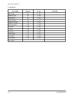
2) ASI510 (SUB)

ITEM NAME

DEFAULT

Range

REMARK

Gamma Red

32

0 ~ 127

Gamma Green

32

0 ~ 127

Gamma Blue

32

0 ~ 127

Sub Color Enable

0

0 ~ 1

Sub Color

16

0 ~ 1

Sharpness Filter 1

0

0 ~ 63

Sharpness Filter 2

0

0 ~ 63

Sharpness Filter 3

0

0 ~ 63

Sharpness Filter 4

0

0 ~ 63

Sharpness Filter 5

0

0 ~ 63

Sharpness Filter 6

0

0 ~ 63

Sharpness Filter 7

0

0 ~ 63

Sharpness Filter 8

0

0 ~ 63

Sharpness Filter 9

0

0 ~ 63

Sharpness Filter 10

0

0 ~ 63

Filter H Limit

3

0 ~ 3

Filter V Limit

3

0 ~ 3

Filter H Chroma Limit

3

0 ~ 3

Filter V Chroma Limit

3

0 ~ 3

Chroma Filter Enable

0

0 ~ 1

Noise Filter 0

0

0 ~ 15

Noise Filter 1

0

0 ~ 15

Noise Filter 2

0

0 ~ 31

Noise Filter 3

0

0 ~ 15

Noise Filter 4

0

0 ~ 15

Noise Filter 5

0

0 ~ 31

Noise Filter 6

0

0 ~ 15

Noise Filter 7

0

0 ~ 15

Noise Filter 8

0

0 ~ 31

Noise Filter Enable

0

0 ~ 1

NR Filter Enable

0

0 ~ 1

Summary of Contents for SP50L3HXX/XEC

Page 1: ...assis M62A P Atlantis_Europe Model SP50L3HXX XEC DLP TV CONTENTS Specifications Alignment and Adjustments Exploded View and Parts List Service Item Block Diagrams Schematic Diagrams 1 2 3 4 5 6 SERVIC...

Page 2: ...Electronics Co Ltd Nov 2004 Printed in Korea AA82 02047A This Service Manual is a property of Samsung Electronics Co Ltd Any unauthorized use of Manual can be punished under applicable International...

Page 3: ...D x H Weight 1094 x 339 x 814 mm 43 07 x 13 35 x 32 05 inches 31 5Kg 69 44 Ibs 35Kg 77 16 Ibs 41 5Kg 91 49 Ibs 45Kg 99 21 Ibs 1182 x 359 x 870 mm 46 54 x 14 13 x 34 25 inches AC100V 240V 50Hz 60Hz 200...

Page 4: ...1 2 Samsung Electronics MEMO...

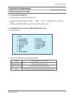
Page 5: ...times of SERVICE MODE Switch overs 2 1 2 A OSD DISPLAY 2 1 2 B BUTTONS OPERATIONS WITHIN SERVICE MODE 2 Alignment and Adjustments MENU Full Menu Display Move to Parent Menu Direction keys Item Selecti...

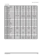
Page 6: ...arpness Filter 5 0 0 63 Sharpness Filter 6 0 0 63 Sharpness Filter 7 0 0 63 Sharpness Filter 8 0 0 63 Sharpness Filter 9 0 0 63 Sharpness Filter 10 0 0 63 Filter H Limit 3 0 3 Filter V Limit 3 0 3 Fil...

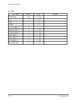
Page 7: ...r 5 0 0 63 Sharpness Filter 6 0 0 63 Sharpness Filter 7 0 0 63 Sharpness Filter 8 0 0 63 Sharpness Filter 9 0 0 63 Sharpness Filter 10 0 0 63 Filter H Limit 3 0 3 Filter V Limit 3 0 3 Filter H Chroma...

Page 8: ...0 OFF ON LUMA DELAY 0 Fixel updated when h 20 SDT is written IF compensation 0 0 3 Off 6dB 12dB 10dB Chroma Bandwidth 1 0 3 narrow normal broad wide Luma LPF Enable 0 OFF ON HPLL SPEED 2 0 3 No chang...

Page 9: ...arrow normal broad wide Luma LPF Enable 0 OFF ON HPLL SPEED 2 0 3 No change Terrestrial VCR Mixed V PEAKING 0 0 15 YUV CONTRAST 27 0 63 480i YPbPr Component mode YUV BRIGHTNESS 70 128 127 YUV SATCB 42...

Page 10: ...E DEFAULT Range REMARK RED GAIN 88 0 255 GREEN GAIN 88 0 255 BLUE GAIN 88 0 255 RED OFFSET 128 0 255 GREEN OFFSET 128 0 255 BLUE OFFSET 128 0 255 PB GAIN 142 0 255 Y GAIN 128 0 255 PR GAIN 142 0 255 P...

Page 11: ...04 128 128 32 220 160 50 10000 120 358 12000 200 358 8 8 12 4 1 1 1 REMARK Test Pattern Selection DNIe Block Enb Bypass Temporal NR Gain Temporal NR Gain Spatial NR Gain NR Mode Selection DE Paramete...

Page 12: ...R2RGB Color Matrix Conversion Coefficient Value YCBCR2RGB Color Matrix Conversion Coefficient Value YCBCR2RGB Color Matrix Conversion Coefficient Value YCBCR2RGB Color Matrix Conversion Coefficient Va...

Page 13: ..._Green y 690 19 D_Green G 1000 20 D_Blue x 147 21 D_Blue y 64 22 D_Blue G 1000 23 D_Cyan x 190 24 D_Cyan y 260 25 D_Cyan G 1000 26 D_Magneta x 277 27 D_Magneta y 131 28 D_Magneta G 1000 29 D_Yellow x...

Page 14: ...1 ITEM NAME DEFAULT Range REMARK V Position 30 0 60 H Position 60 0 120 LAMP 2 0 4 Index delay 48 40 0 1023 Seq Select 5 3 0 15 V Flip Normal 0 1 H Flip Normal 0 1 Gamma 2 0 15 SLR 0 0 1 DMD Bias 3 0...

Page 15: ...10 SCALE_NOISE_Y 30 0 255 SCALE_NOISE_C 100 0 255 DEP_GAIN2_X 4 0 255 DEP_GAIN2_Y 4 0 255 DEP_GAIN3_X 01 0 255 DNIe_DEP_GAIN 30 0 255 RF_DB 2 ITEM NAME DEFAULT Range REMARK BASE LEVEL 230 0 1024 PK 1...

Page 16: ...onics RF_DB 3 ITEM NAME DEFAULT Range REMARK BASE LEVEL 650 0 1024 PK 0 0 7 LPF2 1 0 3 PKCOR 0 0 1 H_P_F_ENABLE 0 0 10 SCALE_NOISE_Y 0 0 255 SCALE_NOISE_C 0 0 255 DEP_GAIN2_X 0 0 255 DEP_GAIN2_Y 0 0 2...

Page 17: ...lignment and Adjustments Samsung Electronics 2 13 11 DDP PATTERNS DDP PATTERNS REMARK White Red Green Blue Cyan Mazenta Yellow H Ramp V Ramp H Lines Diagonal Lines V Lines Grid Checkerboard V frequenc...

Page 18: ...d Adjustments 2 14 Samsung Electronics 12 ASI PATTERNS ITEM NAME DEFAULT Range REMARK CROSS BAR CROSS HATCH CHECKER CHARACTER BOX STEP 64 STEP 32 STEP 16 STEP 8 COLOR BAR FILKER_100 FILKER_75 FILKER_5...

Page 19: ...ast Memory 10 High Deviation On On Off Off 11 Carrier Mute On Off On On 12 Auto Power On On On On 13 DNIe Demo On On On On 14 Melody Volume 0 20 5 5 5 15 DDC Write Enable On Off Off Off 16 Plug Play O...

Page 20: ...Alignment and Adjustments 2 16 Samsung Electronics 2 1 4 CCA Adjustment Service Methods 1 Condition of the CCA Label upon Receipt of the Service Engine...

Page 21: ...suring that you adjust until you get the OK sign After adjusting exit Factory Mode 6 When the adjustment is complete check the picture quality If necessary change the D White x y values to the desired...

Page 22: ...e the actuator values to eliminate saw tooth shapes from the A and B areas To fine tune increase the data value ensuring that you get the center between the starting and ending points of the disappear...

Page 23: ...Samsung Electronics 2 19 Alignment and Adjustment 2 2 Contents Failure Repair Methods...

Page 24: ...Alignment and Adjustments 2 20 Samsung Electronics...

Page 25: ...Alignment and Adjustments Samsung Electronics 2 21...

Page 26: ...Alignment and Adjustments 2 22 Samsung Electronics...

Page 27: ...Alignment and Adjustments Samsung Electronics 2 23...

Page 28: ...Alignment and Adjustments 2 24 Samsung Electronics 2 3 ASSY PCB ANALOG Service Manual...

Page 29: ...Alignment and Adjustments Samsung Electronics 2 25...

Page 30: ...Alignment and Adjustments 2 26 Samsung Electronics...

Page 31: ...Alignment and Adjustments Samsung Electronics 2 27...

Page 32: ...Alignment and Adjustments 2 28 Samsung Electronics 2 4 ASSY PCB DIGITAL Service Manual...

Page 33: ...Alignment and Adjustments Samsung Electronics 2 29 2 4 1 Digital Board Characteristics...

Page 34: ...Alignment and Adjustments 2 30 Samsung Electronics...

Page 35: ...Alignment and Adjustments Samsung Electronics 2 31 2 5 ASSY PCB DMD Service Manual...

Page 36: ...Alignment and Adjustments 2 32 Samsung Electronics...

Page 37: ...Alignment and Adjustments Samsung Electronics 2 33...

Page 38: ...Alignment and Adjustments 2 34 Samsung Electronics...

Page 39: ...Alignment and Adjustments Samsung Electronics 2 35...

Page 40: ...Alignment and Adjustments 2 36 Samsung Electronics...

Page 41: ...Alignment and Adjustments Samsung Electronics 2 37 2 6 ASSY PCB POWER Service Manual...

Page 42: ...Alignment and Adjustments 2 38 Samsung Electronics 2 7 Troubleshooting...

Page 43: ...Alignment and Adjustments Samsung Electronics 2 39...

Page 44: ...Alignment and Adjustments 2 40 Samsung Electronics...

Page 45: ...Alignment and Adjustments Samsung Electronics 2 41...

Page 46: ...Alignment and Adjustments 2 42 Samsung Electronics...

Page 47: ...Alignment and Adjustments Samsung Electronics 2 43...

Page 48: ...the more advanced features you must use the remote control Switch among video input modes Display the on screen menu Select the channels Adjust the volume Access to the selected option on the menu sys...

Page 49: ...or Off is selected Air vent cover in the rear of the TV is not properly installed Inside temperature of the TV is over normal Clean the air vent cover in the rear of the TV Turn the TV back on after 1...

Page 50: ...nics 2 11 Remote Control You can use the remote control up to about 23 feet from the TV When using the remote control always point it directly at the TV You can also use your remote control to operate...

Page 51: ...0902 BN96 01187A ASSY MISC P BRKT MIRROR 50L3 SECC 1 S N A T0260 BP67 00096A MIRROR MIRROR FRONT 50 GLASS 1100X580X5 1 T0264 BP60 00032L SPACER MIRROR 50L3 EVA 490 T1 0 28 4 S N A T0928 BP61 00537A BR...

Page 52: ...Exploded View Parts List 3 2 Samsung Electronics 3 2 Exploded View of Engine...

Page 53: ...Exploded View Parts List Samsung Electronics 3 3 50 61 Optical materials...

Page 54: ...1T 1 T0053 BP67 00109A SCREEN FRESNEL 50W 1126 646 2T 1 T0027 BP94 00484A ASSY PCB S DMD HLP5063WX XAA L62B ATLANT 1 S N A T0269 BP94 00485A ASSY PCB S ACTUATOR SUB DETECT HLP5063WX 1 T0091 BP94 0214...

Page 55: ...Service Item 4 2 Samsung Electronics MEMO...

Page 56: ...Diagram 5 1 Analog Board PCB Layout 2 0mm 30p 26 2 0mm 7p 26 2 0mm 9p 26 2 0mm 10p 26 2 0mm 6p 26 2 0mm 3p 26 2 0mm 32p 26 2 5mm 5p 22 2 5mm 5p 22 2 5mm 13p 22 2 5mm 11p 26 2 5mm 6p 22 This Document c...

Page 57: ...ler D CPU Scaler D TV D TV D VI VI DNIe L DNIe LVD VDS Blo lock ck Po Po we wer Block lock 245mm L V D S O U T P U T 2R 30P 2mm Blk 2R 30P 2mm Blk AV Signals 6P 2 5mm 6P 2 5mm Power 2R 32P 2mm Blk 2R...

Page 58: ...D A e t a t S i r T W S r e x i M T U O Y N I A M T U O C N I A M T U O Y B U S T U O C B U S V Y N I A M C N I A M C B U S T U O Y V B U S T U O V X T T T U O V N O M T U O V T V T U O T X E 2 2 4 6...

Page 59: ...MEMO 5 4 Samsung Electronics...

Page 60: ...A R O T C E T E D B U S O T D R A O B D M D O T 2 3 7 C V 5 3 F u 0 0 1 m h o K 0 1 2 1 9 R W 0 1 1 W 0 1 1 1 1 9 R m h o K 2 6 0 6 7 R m h o 5 4 8 W 0 1 1 m h o K 1 5 W 0 1 1 2 6 7 R W 0 1 1 m h o K...

Page 61: ...u T e h t e s U 1 0 2 U T R E T T I L P S F R 3 0 2 U T A 0 3 1 0 0 0 4 A A X s w o l l o f s a 5 4 5 C 4 4 5 C e s U N I A M X r e t t i l p S 2 2 2 N C l a n o i t i d d a e s U S U C S T N n I R E...

Page 62: ...T U O R 1 T X E R 1 P M O C C D E R 2 T X E T U O R 2 T X E N I L 1 T X E U L B 3 T X E L 1 P M O C R L V _ 1 V 1 A C R C S T N N I L 3 T X E N I L 2 V L 2 P M O C T E D 2 V T E D 2 T X E T U O V 3 T...

Page 63: ...0 0 1 2 9 9 R 0 W 6 1 1 0 9 0 1 R W 6 1 1 0 3 2 1 1 R 3 9 0 1 R W 6 1 1 0 K 7 4 W 6 1 1 L A I R E T A M V 5 2 F n 0 0 1 0 7 7 C 4 6 0 1 R W 6 1 1 0 0 1 W 6 1 1 0 3 9 9 R 0 F u 0 1 V 6 1 3 7 6 C B 5 8...

Page 64: ...1 1 R W 0 1 1 C N 5 N I _ M 6 T U O 7 D N G 8 9 D N G MGND1 MGND1 MGND2 MGND2 5 1 1 T F 3 4 2 5 K K S L 5 5 3 H T 1 C N 0 1 D N G 2 N I 3 T U O _ M C N 4 m h o K 9 3 2 8 1 1 R W 0 1 1 C N 6 N I _ M 7...

Page 65: ...O T 8 5 0 1 R 9 5 0 1 R 1 N I A G Q E _ L B J _ O T _ L T U P N I Q E _ L B J _ O T _ R T U P N I B V 9 Q E _ L B J _ M O R F _ L T U P T U O Q E _ L B J _ M O R F _ R T U P T U O R T U P T U O 0 N I...

Page 66: ...1 V 6 1 F u 0 1 8 0 7 C 9 9 0 1 R 0 7 4 1 16W 1 16W V 6 1 F u 0 1 0 1 7 C K 1 W 6 1 1 7 3 9 R B V 9 5 4 9 R K 1 W 6 1 1 8 3 9 R W 6 1 1 K 1 5 3 9 R W 6 1 1 K 1 4 5 7 C 9 3 9 R V 6 1 F u 2 2 K 1 W 6 1...

Page 67: ...u t c A 4 2 Y E K 3 3 2 2 D E L 5 3 D E L 6 D N G 2 A V 5 3 T E N I B A C 7 L R I 1 D N G 7 B 2 2 Y E K 3 1 C B A 3 L n o i t c e n n o C l a n g i S r e d n a p x E O I M A D S 4 M L C S 5 1 D E L 1...

Page 68: ...5 2 6 2 7 2 8 2 9 3 3 0 1 1 1 2 1 3 1 4 1 5 1 6 1 7 1 8 1 9 2 2 0 1 1 0 3 2 4 5 6 7 8 9 2 3 2 4 2 5 2 6 2 7 2 8 2 9 3 3 0 3 1 1 3 1 4 1 5 1 6 1 7 1 8 1 9 2 2 0 2 1 2 2 1 1 0 1 1 1 2 This Document can...

Page 69: ...C 15 16 VDD 2 0Y 3 1Z 4 Z COM 5 0Z 6 INH VEE 7 1 1Y B 10 11 A 0X 12 13 1X X COM 14 Y COM IC103 74VHC4053MX 2 GND 3 B0 4 A VCC 5 6 S NC7SB3157P6X IC102 1 B1 47nF 16V C253 This Document can not be used...

Page 70: ...Samsung Electronics Schematic Diagrams 6 11 13 5MHz This Document can not be used without Samsung s authorization 6 2 3 FLI2310_MAIN...

Page 71: ...ectronics A 4 5 VCC S 6 B1 1 GND 2 B0 3 4 0Z 5 INH 6 7 VEE VSS 8 C 9 11 12 0X 1X 13 14 X COM 15 Y COM VDD 16 0Y 2 1Z 3 Z COM 74VHC4053MX IC100 1Y 1 10 B A This Document can not be used without Samsung...

Page 72: ...Samsung Electronics Schematic Diagrams 6 13 This Document can not be used without Samsung s authorization 6 2 5 CXA2171...

Page 73: ...4 N I U L B 3 4 D N G 4 4 D D V A 5 4 D D V A 6 4 D N G 7 4 N I N R G 8 4 N I G O S 34 34 AVDD AVDD 35 35 GND GND 36 36 MIDSCV MIDSCV 37 37 CLAMP CLAMP 38 38 AVDD AVDD 39 39 5 G 4 GND GND 40 40 D N G...

Page 74: ...7 8 1 2 3 4 5 6 2 3 4 5 6 7 8 1 1 2 3 4 5 6 7 8 1 2 3 4 5 6 7 8 4 5 6 7 8 1 2 3 1 2 3 4 5 6 7 8 MGND2 MGND2 MGND3 MGND3 MGND4 MGND4 9 1 2 3 4 5 6 7 8 9 MGND1 MGND1 1 0 1 1 1 2 1 3 1 4 1 5 1 6 1 7 1 8...

Page 75: ...Schematic Diagrams 6 16 Samsung Electronics C C V 8 0 G 1 T C H A 4 7 2 5 1 C I 1 B 2 A 3 D N G 4 Y 5 This Document can not be used without Samsung s authorization 6 2 8 LVDS_OUTPUT...

Page 76: ...Electronics Schematic Diagrams 6 17 2 E 3 4 S S V 5 A D S L C S 6 7 C W C C V 8 1 0 1 C I 7 2 C S 0 1 N 4 6 C 4 2 T A 0 E 1 1 E 2 This Document can not be used without Samsung s authorization 6 2 9 S...

Page 77: ...ams 6 18 Samsung Electronics 9 4 1 2 1 D 3 1 O 2 E O 4 2 D 5 2 O 6 7 D N G 8 3 O 3 D 1 1 E O 0 1 3 E O 4 O 1 1 2 1 4 D 4 E O 3 1 C C V This Document can not be used without Samsung s authorization 6 2...

Page 78: ...1 D1 C2 C2 D3 D3 F4 F4 D2 D2 G4 G4 E2 E2 3 1 U 3 1 W 3 1 Y 8 W 9 U 8 V 7 Y 7 W 6 Y 8 U 7 V 0 1 V 9 Y 0 1 U 9 W 9 V 8 Y 4 1 V 5 1 Y 4 1 W 3 1 V 4 1 Y 5 1 U 8 1 Y 7 1 Y 5 1 V 6 1 W 6 1 Y 5 1 W 4 1 U 0 1...

Page 79: ...Samsung Electronics Schematic Diagrams 6 20 6 2 11 DNIe_Pro This Document can not be used without Samsung s authorization...

Page 80: ...OE 40 RA6 RA5 41 42 RA4 RA3 43 44 GND RA2 45 46 RA1 RA0 32 33 RB5 RB4 34 RB3 35 36 RB2 VCC 37 38 RB1 RB0 39 4 25 RC4 RC3 26 27 RC2 RC1 28 29 RC0 PD 3 GND 30 31 CLKOUT RB6 18 19 RD2 2 TEST RD1 20 21 R...

Page 81: ...ON R USE SUBDETECT INSTALL 1Mohm 1 10W R847 R846 1Mohm 1 10W A 2 GND 3 Y 4 VCC 5 IC812 OE 1 8 CS 9 19 2 DB6 20 DGND 3 DB5 DB4 4 DB3 5 DB2 6 7 DB1 DB0 11 12 PD LDAC 13 14 CLR 15 VDD REFIN 16 17 AGND NC...

Page 82: ...Schematic Diagrams 6 22 Samsung Electronics This Document can not be used without Samsung s authorization 6 3 3 FLASH...

Page 83: ...REQUIRED FO R SMALL COL OR WHEELS SEE CUSTOMER ENGINEERING USE 2203 005249 DO NO T INST ALL A 2 GND 3 Y 4 VCC 5 IC810 OE 1 4 Y 5 VCC IC809 1 OE 2 A 3 GND A 3 GND 4 Y 5 VCC IC811 1 OE 2 47Kohm R861 1 1...

Page 84: ...Schematic Diagrams 6 24 Samsung Electronics This Document can not be used without Samsung s authorization 6 3 5 DMD...

Page 85: ...Samsung Electronics Schematic Diagrams 6 25 This Document can not be used without Samsung s authorization 6 3 6 CW...

Page 86: ...100K ohm 1 10W 1 10W R146 R146 100Kohm 100K ohm R140 R140 10Kohm 10K ohm 1 10W 1 10W R145 R145 100Kohm 100K ohm 1 10W 1 10W 1 2W 1 2W 100ohm 100ohm R147 R147 1 2W 1 2W 100ohm 100ohm R139 R139 1 2W 1...

Page 87: ...Schematic Diagrams 6 28 Samsung Electronics This Document can not be used without Samsung s authorization 6 5 POWER...

Page 88: ...Samsung Electronics Schematic Diagrams 6 29 This Document can not be used without Samsung s authorization 6 6 LINE FILTER...

Reviews: