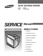


PROJECTION TV RECEIVER
Chassis :
P55A(N) REV.1
Model:
ST55W3PCX/XAX
PROJECTION TV RECEIVER
C O N T E N T S
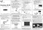
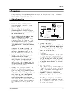
Precautions
Reference Information
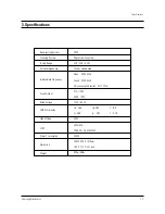
Specifications
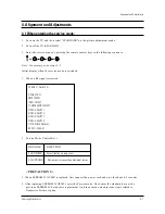
Alignment and Adjustments
Troubleshooting
Exploded View and Parts List
Electric Parts List
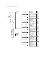
Block Diagrams
Wiring Diagram
Schematic Diagrams
1.
2.
3.
4.
5.
6.
7.
8.
9.
10.
Summary of Contents for ST55W3PCX/XAX
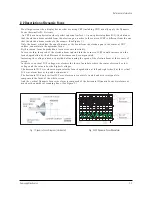
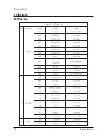
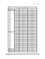
Page 10: ...Reference Information 2 4 Samsung Electronics 2 3 IC Line Up 2 3 1 Progressive ...
Page 11: ...Reference Information Samsung Electronics 2 5 ...
Page 12: ...Reference Information 2 6 Samsung Electronics 2 4 MICOM IIC BUS LINE UP ...
Page 14: ...MEMO 3 2 Samsung Electronics ...
Page 52: ...MEMO 4 38 Samsung Electronics ...
Page 56: ...MEMO 5 4 Samsung Electronics ...
Page 87: ...Schematic Diagrams 10 2 Samsung Electronics TP20 TP03 TP04 10 2 MAIN 2 TP03 TP04 TP20 ...
Page 88: ...Samsung Electronics Schematic Diagrams 10 3 10 3 MAIN 3 TP12 TP13 TP12 TP13 ...
Page 90: ...Samsung Electronics Schematic Diagrams 10 5 10 5 MICOM ...
Page 91: ...Schematic Diagrams 10 6 Samsung Electronics 10 6 CRT ...
Page 92: ...Samsung Electronics Schematic Diagrams 10 7 10 7 SUB 1 TP21 TP21 ...
Page 93: ...Schematic Diagrams 10 8 Samsung Electronics 10 8 SUB 2 TP24 TP23 TP22 TP22 TP23 TP24 ...
Page 94: ...Samsung Electronics Schematic Diagrams 10 9 10 9 CONVERGENCE SDC12 1 ...
Page 95: ...Schematic Diagrams 10 10 Samsung Electronics 10 10 CONVERGENCE SDC12 2 ...
Page 96: ...Samsung Electronics Schematic Diagrams 10 11 10 11 PRO SCAN 1 ...
Page 97: ...Schematic Diagrams 10 12 Samsung Electronics 10 12 PRO SCAN 2 ...
Page 98: ...Samsung Electronics Schematic Diagrams 10 13 10 13 PRO SCAN 3 ...
Page 99: ...Schematic Diagrams 10 14 Samsung Electronics 10 14 PRO SCAN 4 ...
Page 100: ...10 15 CG AMP Samsung Electronics Schematic Diagrams 10 15 ...
Page 101: ...Schematic Diagrams 10 16 Samsung Electronics 10 16 AV FRONT ...
Page 102: ...10 17 CONTROL Samsung Electronics Schematic Diagrams 10 17 ...
Page 103: ...Schematic Diagrams 10 18 Samsung Electronics 10 18 DY JACK SENSOR DY JACK SENSOR ...