Alignment and Adjustment
Samsung Electronics
2-5
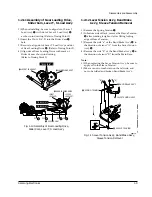
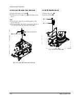
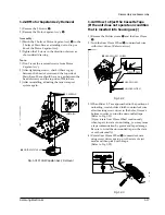
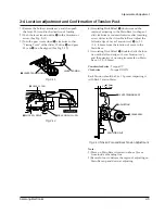
4) As rotating Disk S Reel
Œ
clockwise and the
region of adjusting in the Main Base (in shape of
slit) clockwise or counterclockwise after inserting
screw driver in the slit on Main Base. Adjust the
left end edge of Lever Tension AssÕy
ˇ
to 1.3
+1.5/-0.5mm from the location of mark in the
Main Base.
5) As rotating Disk S Reel
Œ
, double-check the loca-
tion of the left end edge of Lever Tension AssÕy
and the quantity of crossing from mark on Main
Base. (+1.0/-0.5mm)
Counterclockwise
: Torque UP
Clockwise
: Torque DOWN
Back Tension should be 56 ± 15g.cm at inspecting it
with Back Tension Meter.
1.0mm
0.5mm
ˇ
LEVER TENSION ASS'Y
Œ
DISK S REEL
´
ADJUSTING
ADJUSTING SLIT
1.3
Fig. 2-13 Tension Pole and Back Tension Adjustment
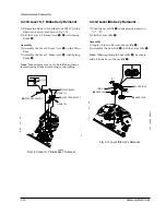
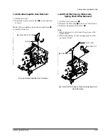
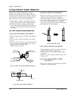
1) Remove the holder cassette assÕy and then push
the lever FL Arm-R to the direction of loading.
2) Push the lever tension drive
Œ
in the direction of
arrow. (See Fig. 2-11)
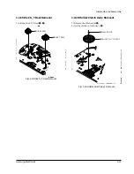
3) Turn the gear worm wheel
´
clockwise so that
ÒTiming PointÓ of the slider FL drive
ˇ
and gear
FL cam
¨
can be aligned (See Fig. 2-12)
Fig. 2-11
Fig. 2-12
¨
GEAR FL CAM
´
GEAR WORM WHEEL
ˇ
SLIDER FL DRIVE
P
TIMING POINT
Œ
LEVER TENSION DRIVE
LEVER TENSION
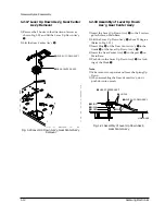
Note
:
1) Mark on Main Base is located in about 1.3mm
from inside of bending line.
2) Be careful not to deform the region of adjusting on
Main Base up and down at adjusting.
2-4 Location adjustment and Confirmation of Tension Post
Summary of Contents for SV-DVD1EA
Page 8: ...Product Specifications 2 2 Samsung Electronics MEMO ...
Page 40: ...Troubleshooting 5 20 Samsung Electronics MEMO ...
Page 50: ...Exploded View and Parts List 6 10 Samsung Electronics MEMO ...
Page 62: ...7 12 Electrical Parts List Samsung Electronics MEMO ...
Page 63: ...Samsung Electronics 8 1 8 Block Diagram ...
Page 64: ...Block Diagram 8 2 Samsung Electronics MEMO ...
Page 66: ...PCB Diagrams 9 2 Samsung Electronics 9 1 S M P S ...
Page 67: ...PCB Diagrams 9 3 Samsung Electronics 9 2 VCR Main ...
Page 68: ...PCB Diagrams 9 4 Samsung Electronics 9 3 DVD Main COMPONENT SIDE SOLDER SIDE ...
Page 69: ...PCB Diagrams 9 5 Samsung Electronics 9 4 Function Timer 9 5 DVD Deck ...
Page 70: ...PCB Diagrams 9 6 Samsung Electronics MEMO ...
Page 71: ...Samsung Electronics 10 1 10 Wiring Diagram ...
Page 72: ...Wiring Diagram 10 2 Samsung Electronics MEMO ...
Page 75: ...Schematic Diagrams 11 3 Samsung Electronics 11 1 S M P S ...
Page 76: ...Schematic Diagrams 11 4 Samsung Electronics 11 2 Power Drive ...
Page 77: ...11 3 Function Timer Schematic Diagrams 11 5 Samsung Electronics ...
Page 78: ...Schematic Diagrams 11 6 Samsung Electronics 11 4 System Control Servo ...
Page 79: ...Schematic Diagrams 11 7 Samsung Electronics 11 5 A V ...
Page 80: ...Schematic Diagrams 11 8 Samsung Electronics 11 6 TM Blcok ...
Page 81: ...Schematic Diagrams 11 9 Samsung Electronics 11 7 Digital Audio ...
Page 82: ...Schematic Diagrams 11 10 Samsung Electronics 11 8 Hi Fi ...
Page 83: ...Schematic Diagrams 11 11 Samsung Electronics 11 9 OSD ...
Page 84: ...Schematic Diagrams 11 12 Samsung Electronics 11 10 Input Output ...
Page 85: ...Schematic Diagrams 11 13 Samsung Electronics 11 11 A2 NICAM ...
Page 86: ...Schematic Diagrams 11 14 Samsung Electronics 11 12 SECAM OPTION ...
Page 87: ...Schematic Diagrams 11 15 Samsung Electronics KEY OPTION 11 13 DVD Main Micom AV Decoder ...
Page 88: ...Schematic Diagrams 11 16 Samsung Electronics 11 14 Servo ...
Page 89: ...Schematic Diagrams 11 17 Samsung Electronics 11 16 DVD Deck ...
Page 90: ...Schematic Diagrams 11 18 Samsung Electronics MEMO ...
Page 115: ...2 6 Samsung Electronics Alignment and Adjustment MEMO ...

