background image

2-8

Alignment and Adjustments

Samsung Electronics

2-3-2 Tape Transport System Adjustment

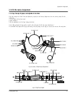
When parts are replaced, perform the required adjustments by referring to procedures for the tape transport
system. If there are any changes to the tape path, first run a T-120 tape and make sure excessive tape wrinkle does
not occur at the tape guides.

If tape wrinkle is observed at the guide roller S, T, turn the guide roller S, T until wrinkle disappears.

If the tape wrinkle is still observed at the tape guide, perform the tilt adjustment of the ACE head.

(1) ACE Head Assembly Adjustment

a.  ACE HEAD HEIGHT ADJUSTMENT   

1) Run the alignment tape (Color bar) in the playback mode.
2) Observe surface of the audio head using a dental mirror.
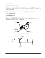
3) Turn screw (C) clockwise or counterclockwise until the gap of lower tape edge and the lower edge of the 

control head is about 0.25mm. (Refer to Fig. 2-10 and 2-11)

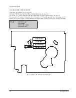
Fig. 2-10 Location of ACE Head Adjustment Screw

Fig. 2-11 ACE Head Height Adjustment

SCREW (A)

TLIT ADJUST

X-POSITION

ADJUSTING SLIT

SCREW (C)
HEIGHT ADJUST

SCREW (D)
X-POSITION LOCKING

SCREW (B)

AZIMUTH ADJUST

0  ~ 0 .25  mm 

AUDIO HEAD

VIDEO HEAD

CONTROL HEAD

Summary of Contents for SV-DVD440P

Page 1: ...40P DVD440P DVD541P DVD546P DVD641P DVD645P SV DVD645P DVD546P SV DVD641P DVD541P DVD440P SV DVD340P AUX AUX ELECTRONICS Samsung Electronics Co Ltd AUG 2004 Printed in Korea AK82 00661A If you want to know additional information which is not included on this Service Manual please refer to the SV DVD440 Training Manual AK82 00513A This Service Manual is a property of Samsung Electronics Co Ltd Any ...

Page 2: ... Motor Load Ass y Separate the Motor Load Ass y 2 When Slider S T approachs the unloading position rotate holder Clutch counterclockwise after inserting screwdriver in the frame s bottom hole in order to wind the unwound tape Refer to Fig 3 If you rotate Gear Worm Œ continuously when tape is unwinding you may cause tape contamination by grease and tape damage Be sure to wind the unwound tape with ...

Page 3: ...erwriters Laboratories UL 1270 40 7 With the instrument s AC switch first in the ON position and then in the OFF position measure from a known earth ground metal water pipe conduit etc to all exposed metal parts of the instrument antennas handle brackets metal cabinets screw heads metallic overlays control shafts etc espe cially any exposed metal parts that offer an electri cal return path to the ...

Page 4: ...nched out of place or frayed wiring Do not change spacing between a component and the printed circuit board Check the AC power cord for damage 5 Components parts and or wiring that appear to have overheated or that are otherwise damaged should be replaced with components parts and or wiring that meet original specifications Additionally determine the cause of overheating and or damage and if neces...

Page 5: ...d lead last 2 The service precautions are indicated or printed on the cabinet chassis or components When servic ing follow the printed or indicated service precau tions and service materials 3 The components used in the unit have a specified flame resistance and dielectric strength When replacing components use components which have the same ratings Components identi fied by shading by or by in th...

Page 6: ...posure of the assem bly 3 Use only a grounded tip soldering iron to solder or unsolder ESD devices 4 Use only an anti static solder removal devices Some solder removal devices not classified as anti static can generate electrical charges suffi cient to damage ESD devices 5 Do not use freon propelled chemicals These can generate electrical charges sufficient to damage ESD devices 6 Do not remove a ...

Page 7: ... sheet This gives them the same ground as the sheet 4 Remove the optical pick up block 5 Perform work on top of the conductive sheet Be careful not to let your clothes or any other static sources to touch the unit Be sure to put on a wrist strap grounded to the sheet Be sure to lay a conductive sheet made of copper etc Which is grounded to the table Fig 1 3 6 Short the short terminal on the PCB wh...

Page 8: ... Assy 3 Make solder land 2 points short on Pick up See Fig 1 4 4 Disassemble the Pick up 1 5 2 Assembly 1 Replace the Pick up 2 Remove the soldering 2 points on Pick up 3 Reassemble the Deck Assy PICK UP ASS Y SOLDER LAND 2 POINTS SHORT Note If the assembly and disassembly are not done in correct sequence the Pick up may be damaged Fig 1 4 ...

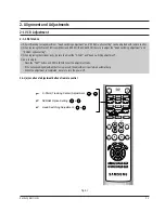
Page 9: ...setting 3 When replacing the cylinder ass y be sure to adjust the X Point and Head switching adjustment 4 How to adjust Press the TEST botton on VCR MAIN PCB to set the adjustment mode If the corresponding adjustment button is pressed the adjustment is performed automatically When the adjustment is completed be sure to turn the power off 2 1 1 a Location of adjustment button of remote control Fig ...

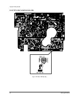
Page 10: ...2 2 Alignment and Adjustments Samsung Electronics 2 1 1 b TEST location for adjustment mode setting Fig 2 2 VCR Main PCB Top View TEST BUTTON ...

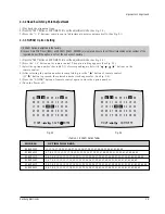
Page 11: ...icom IC601 and NVRAM IC603 EEPROM are replaced be sure to set the corresponding option number of the required model If the option is not set the unit will not operate MOVE SAVE ENTER 01 02 03 04 05 06 07 08 09 10 11 12 13 14 15 16 17 18 19 20 21 22 23 24 25 26 27 28 29 30 31 32 33 34 35 36 37 38 39 40 Fig 2 3 MOVE COMPLETE 01 02 03 04 05 06 07 08 09 10 11 12 13 14 15 16 17 18 19 20 21 22 23 24 25 ...

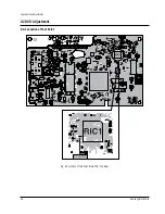
Page 12: ...2 4 Alignment and Adjustments Samsung Electronics 2 2 DVD Adjustment 2 2 1 Location of Test Point Fig 2 5 Location of test Point Main PCB Top Side Pin 29 of RIC1 ...

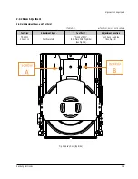
Page 13: ...nd Test Point 2 2 2 Skew Adjustment Test Disc Adjustment Spec Test Point Adjustment Location TDV 533 Pin 29 of RIC1 Ass y Deck Top Side Chapter 14 Flat Waveform DVD Main PCB Top Side See Fig 2 6 See Fig 2 5 Fig 2 6 Ass y Deck Top Side Test Disc Service not Available Table 2 2 ...

Page 14: ...et the Oscilloscope Range as follows Voltage 50mV Div Frequency 10m Sec 3 Adjust the Screws A and B See Fig 2 6 using a Hex screwdriver until you obtain a Flat Waveform and the picture is stable Then go to Chapter 1 and make sure the Waveform is Flat here as well If not you have to go back to Chapter 14 and adjust again If you cannot obtain a Flat waveform then the unit is defective Note The Deck ...

Page 15: ...eference for the transport adjustment To maintain the height of the tape guide and prevent damage do not apply excessive force onto the main base Fig 2 8 Location of Tape Transport Adjustment Fig 2 9 Tape Travel Diagram CYLINDER ASS Y TAKE UP REEL DISK 8 GUIDE POST 9 GUIDE POST SUPPLY REEL DISK CAPSTAN PINCH ROLLER GUIDE ROLLER T GUIDE ROLLER S FULL ERASE HEAD 3 GUIDE POST TENSION POST HEIGHT SCRE...

Page 16: ...e is still observed at the tape guide perform the tilt adjustment of the ACE head 1 ACE Head Assembly Adjustment a ACE HEAD HEIGHT ADJUSTMENT 1 Run the alignment tape Color bar in the playback mode 2 Observe surface of the audio head using a dental mirror 3 Turn screw C clockwise or counterclockwise until the gap of lower tape edge and the lower edge of the control head is about 0 25mm Refer to Fi...

Page 17: ...wer flange of tape guide as shown in Fig 2 12 B 3 If a curl or wrinkle of the tape occurs slightly turn the screw A tilt adjust on the ACE head ass y 4 Reconfirm the ACE head height Fig 2 12 Tape Guide Check c AUDIO AZIMUTH ADJUSTMENT 1 Load alignment tape Mono scope and playback the 7KHz signal 2 Connect channel 1 scope probe to audio output 3 Adjust screw B to achieve maximum audio level See Fig...

Page 18: ...s then adjustment is operates automatically See Fig 2 1 4 Connect the CH 1 probe to Envelope the CH 2 probe to H D switching pulse and then trigger to CH 1 5 Insert the driver into the X Point adjustment hole and adjust it so that envelope waveform is maximum Test point W325 Audio Output W324 Envelope W323 H D S W Trigger W322 Control Pulse Fig 2 13 Location of Test point VCR Main PCB Top View AUD...

Page 19: ... follows Note a Maximum output of the video RF envelope b Minimum output of the video RF envelope at the entrance side c Minimum output of the video RF envelope at the center point d Maximum output of the video RF envelope at the exit side 4 If the section A in Fig 2 15 does not meet the specification adjust the guide roller S up or down 5 If the section B in Fig 2 15 does not meet the specificati...

Page 20: ...ope CH 1 to the Envelope and CH 2 to the H D SW Pulse for triggering 8 Turn the guide roller heads with a flat head driver to obtain a flat video RF envelope as shown in Fig 2 16 Fig 2 16 Guide Roller S T Height Adjustment IDEAL ENVELOPE SHEIGHTTOOHIGH SHEIGHTTOOLOW THEIGHTTOOHIGH THEIGHTTOOLOW GUIDE ROLLER S GUIDE ROLLER T ...

Page 21: ...E Fig 2 17 Video Envelope Rising when Operation mode Changes from RPS to Play Mode 4 Envelope Check 1 Make recordings on T 120 E 120 and T 160 E 180 tape Make sure the playback output envelope meets the specification as shown in Fig 2 18 2 Play back a self recorded tape recording made on the unit using with T 120 E 120 The video envelope should meet the specification as shown in Fig 2 18 In SP mod...

Page 22: ... ass y drives the disk reel S T through gear idler by rotation of gear center ass y 3 Brake is operated by slider cam at FF REW mode 4 Transportation of accurate driving force is done by gears Gear Center Ass y Note If the spec does not meet the followings specifications replace the holder clutch ass y and then recheck MODE TORQUE g cm GAUGE PB 42 11 Cassette Torquemeter RPS 145 30 Cassette Torque...

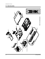
Page 23: ...rts List 3 1 Cabinet Assembly 3 2 3 2 VCR Mechanical Parts Top Side 3 4 3 3 VCR Mechanical Parts Bottom Side 3 6 3 4 DVD Mechanical Parts 3 8 You can search for the updated part code through ITSELF web site URL http itself sec samsung co kr Notice ...

Page 24: ...Exploded View and Parts List 3 2 Samsung Electronics 3 1 Cabinet Assembly W202 W252 A001 C015 W001 P002 P021 P020 C001 C003 C012 W202 C011 C002 P001 LD61A S602A P025 ...

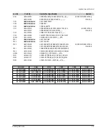
Page 25: ...7 00814B ASSY CONNECTOR BOARD HIPS 94HB DVD V340 SV DVD340P DVD440P Only AK97 00814A ASSY CONNECTOR BOARD HIPS DVD V540 XSA Other Only P021 AK61 00320A CONNECTOR BOARD SV DVD340 XEF HIPS 94HB P025 AC39 10019A CBF POWER CORD KKP 419C H03VVH2 F VDE KE S602A AC61 00341A HOLDER TR X 11 POM K300 NTR W001 6003 000275 SCREW TAPTITE BH B M3 L10 BLK SWCH101 W202 6003 000277 SCREW TAPTITE BH B M3 L12 ZPC YE...

Page 26: ...t 3 4 Samsung Electronics 3 2 VCR Mechanical Parts Top Side G001 G555 G510 G480 K546 B410 B440 B411 B448 B452 G546 G060 G520 G527 K188 K182 K110 K240 K248 K350 K330 K140 K340 G070 K470 B474 B473 K250 K530 K490 G530 G420 G450 K502 ...

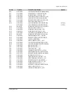
Page 27: ...10 6006 001075 SCREW ASS Y TAPT WSP PH M2 6 L5 0 ZPC G520 AC66 00074A LEVER GUIDE 9 TS 9 PPS BLK KHA G527 AC61 60553A SPRING ETC GUIDE 9 X 9 SUS304 WPB 0 25 G530 AC33 00007A HEAD FE HVFHPOO43A G546 AC66 00005A LEVER FL DOOR TS 10 POM NAT G555 AC97 02293A ASSY UNIT PINCH SECC SUS304 TS 10 FOR X G560 AC97 02215A ASSY POST 8 GUIDE SUS303 POM M90 44 EQ K110 AC66 10267A REEL DISK S X 9 POM K140 AC66 10...

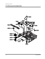
Page 28: ...Exploded View and Parts List 3 6 Samsung Electronics 3 3 VCR Mechanical Parts Bottom Side G542 B462 B560 B484 B488 B475 B500 B456 B458 B464 B468 K222 K200 K225 K221 B478 B570 B460 ...

Page 29: ...5 AC66 00085A DAMPER CAPSTAN X 11 POM M90 44 B478 AC66 00016A LEVER TENSION DRIVE TS 10 SECC E20 20 1 B484 AC66 00078A GEAR LOADING DRIVE X 11 POM K300 B488 AC97 02195A ASSY LEVER LOADING S SECC POM SUS X 11 F B500 AC97 02196A ASSY LEVER LOADING T SECC POM SUS X 11 F B560 AC81 00004A MOTOR CAPSTAN THRUST END PLAY 0 2 MR FG B570 AC60 10514A SCREW CAPSTAN M2 6 L6 PH G542 AC66 60051A BELT PULLEY 5CM ...

Page 30: ...loded View and Parts List 3 8 Samsung Electronics 3 4 DVD Mechanical Parts H212 H205 H210 H209 H903 H104 H109 H106 H105 H107 H207 H206 H904 H904 H211 H206 H203 H103 H108 H204 H903 H903 H241 H102 H202 H900 ...

Page 31: ...P 15 COMBO H202 AK73 00005B RUBBER INSULATOR DP 15 BUTYL 12 HS30 H H203 AH61 50327A SHAFT P U DP 3 SUS L84 7 OD3 H204 AK66 00043A GEAR FEED A DP 15 POM H205 AK66 00044A GEAR FEED B DP 15 POM H206 AK61 00032A HOLDER CAM SKEW DP 9 POM BLACK H207 AK31 00014A MOTOR SPINDLE DP 15 3000RPM H209 AK64 00491A CHASSIS SUB DP 15 POM H210 AK31 00005A MOTOR FEED ASSY DP 9 H211 AK97 00638A ASSY PICK UP SOH DT2 T...

Page 32: ...203 005148 C CER CHIP 100nF 10 16V X7R TP 1608 C332 2203 000975 C CER CHIP 47nF 10 25V X7R TP 1608 C333 2401 000408 C AL 10uF 20 16V GP TP 3 5x5 2 5 C334 2203 000975 C CER CHIP 47nF 10 25V X7R TP 1608 C334A 2203 000236 C CER CHIP 0 1NF 5 50V C0G TP 1608 C335 2203 001652 C CER CHIP 470nF 80 20 16V Y5V TP 1608 C336 2203 000975 C CER CHIP 47nF 10 25V X7R TP 1608 C337 2203 001652 C CER CHIP 470nF 80 2...

Page 33: ... CER CHIP 1nF 10 50V X7R TP 1608 C706 2203 000239 C CER CHIP 0 1NF 5 50V C0G TP 2012 C707 2401 001992 C AL 2200UF 20 10V WT TP 10X20MM 5 C708A 2203 000257 C CER CHIP 10nF 10 50V X7R TP 1608 C714 2203 000491 C CER CHIP 2 2nF 10 50V X7R TP 1608 C818 2203 000783 C CER CHIP 0 33NF 5 50V C0G TP 1608 C819 2203 000783 C CER CHIP 0 33NF 5 50V C0G TP 1608 C820 2203 000783 C CER CHIP 0 33NF 5 50V C0G TP 160...

Page 34: ...TO Q1P111 0501 000362 TR SMALL SIGNAL KSC2328A Y NPN 1000MW TO Q301F 0501 000002 TR SMALL SIGNAL KSA812 PNP 150MW SOT 23 Q302 0501 000341 TR SMALL SIGNAL KSC1623 L NPN 200mW SOT Q3A01 0501 000398 TR SMALL SIGNAL KSC945 NPN 250mW TO 92 T Q3A02 0501 000303 TR SMALL SIGNAL KSA733 PNP 250mW TO 92 T Q3A03 0501 000442 TR SMALL SIGNAL KTC3203 Y NPN 400mW T0 9 Q3A04 0501 000442 TR SMALL SIGNAL KTC3203 Y N...

Page 35: ...1 2001 000515 R CARBON 220OHM 5 1 8W AA TP 1 8X3 2MM R642 2001 000515 R CARBON 220OHM 5 1 8W AA TP 1 8X3 2MM R643 2007 000084 R CHIP 4 7Kohm 5 1 10W TP 1608 R651 2001 000010 R CARBON 68KOHM 5 1 8W AA TP 1 8X3 2MM R652 2001 000568 R CARBON 27OHM 5 1 8W AA TP 1 8X3 2MM R657 2007 000100 R CHIP 68Kohm 5 1 10W TP 1608 R660 2001 000786 R CARBON 47KOHM 5 1 8W AA TP 1 8X3 2MM R661 2001 000660 R CARBON 33K...

Page 36: ...Y5P TP 8 5 C1SS06 2201 002044 C CERAMIC DISC 0 1NF 10 400V Y5P TP 8 5 C1SS10 2401 003303 C AL 82uF 20 400V GP BK 22X30 10 C1SS11 2401 000598 C AL 1uF 20 50V GP TP 4x7 5 C1SS12 2401 002299 C AL 4 7uF 20 50V GP TP 5x7 5 C1SS15 2401 001992 C AL 2200UF 20 10V WT TP 10X20MM 5 C1SS16 2401 003480 C AL 1000UF 20 10V LZ TP 10X16MM 5 C1SS17 2401 001992 C AL 2200UF 20 10V WT TP 10X20MM 5 C1SS18 2401 001992 C...

Page 37: ...5 2 5 C508 2203 000888 C CER CHIP 4 7nF 10 50V X7R TP 1608 C510 2401 001502 C AL 47uF 20 16V GP TP 6 3x5 2 5 C511 2203 000257 C CER CHIP 10nF 10 50V X7R TP 1608 C513 2203 000257 C CER CHIP 10nF 10 50V X7R TP 1608 C517 2203 000888 C CER CHIP 4 7nF 10 50V X7R TP 1608 C518 2401 000909 C AL 22uF 20 16V GP TP 5x5 2 5 C519 2203 000257 C CER CHIP 10nF 10 50V X7R TP 1608 C520 2401 001249 C AL 4 7uF 20 35V...

Page 38: ...ODE SWITCHING 1N4148 75V 150MA DO 35 T D703 0401 000101 DIODE SWITCHING 1N4148 75V 150MA DO 35 T D704 0401 000101 DIODE SWITCHING 1N4148 75V 150MA DO 35 T D705 0401 000101 DIODE SWITCHING 1N4148 75V 150MA DO 35 T D805 0401 000101 DIODE SWITCHING 1N4148 75V 150MA DO 35 T DT701 AC07 00069A LED DISPLAY BCD 9027E SV DVD440 5 DIGIT F1SS01 3601 001123 FUSE CARTRIDGE 250V 1 6A TIME LAG CERAMI FL3A01 2702...

Page 39: ...8x3 2mm R1SS35 2004 000459 R METAL 2 2Kohm 1 1 8W AA TP 1 8x3 2m R301F 2007 000075 R CHIP 220ohm 5 1 10W TP 1608 R302F 2007 000075 R CHIP 220ohm 5 1 10W TP 1608 R315 2007 000122 R CHIP 1 2Kohm 5 1 10W TP 1608 R316 2007 001179 R CHIP 8 2Kohm 5 1 10W TP 1608 R320 2007 000458 R CHIP 18Kohm 5 1 10W TP 1608 R321 2007 000090 R CHIP 10Kohm 5 1 10W TP 1608 R322 2007 000458 R CHIP 18Kohm 5 1 10W TP 1608 R3...

Page 40: ...P 1608 R679 2007 000075 R CHIP 220ohm 5 1 10W TP 1608 R682 2007 000094 R CHIP 22Kohm 5 1 10W TP 1608 R685 2001 000812 R CARBON 5 6KOHM 5 1 8W AA TP 1 8X3 2M R688 2007 000129 R CHIP 27Kohm 5 1 10W TP 1608 R691 2007 000075 R CHIP 220ohm 5 1 10W TP 1608 R693 2007 000097 R CHIP 47Kohm 5 1 10W TP 1608 R694 2007 000097 R CHIP 47Kohm 5 1 10W TP 1608 R698 2001 000290 R CARBON 10KOHM 5 1 8W AA TP 1 8X3 2MM...

Page 41: ...3MIL DUAL 100V m AL1 3301 001419 BEAD SMD 220 500 TP 0 3 AL2 3301 001419 BEAD SMD 220 500 TP 0 3 AL3 3301 001419 BEAD SMD 220 500 TP 0 3 AL4 3301 001419 BEAD SMD 220 500 TP 0 3 AQ1 0504 000128 TR DIGITAL NPN 200MW 22K 22K SOT 23 TP AQ2 0504 000156 TR DIGITAL KSR2103 PNP 200MW 22K 22K SOT AQ20 0504 000128 TR DIGITAL NPN 200MW 22K 22K SOT 23 TP AQ21 0504 000156 TR DIGITAL KSR2103 PNP 200MW 22K 22K S...

Page 42: ... TP 1608 DOIC2 3707 001065 CONNECTOR OPTICAL PLUG GP1FA5 Not used SV DVD340P 440P DRIC1 1003 001735 IC MOTOR DRIVER FAN8026G3 SSOPH 28P 18 4 DY1 2801 004279 CRYSTAL UNIT 27 00MHz 10ppm 28 AAA 20pF ECC1 2203 005148 C CER CHIP 100nF 10 16V X7R TP 1608 ECC2 2203 005148 C CER CHIP 100nF 10 16V X7R TP 1608 FB2 3301 001419 BEAD SMD 220 500 TP 0 3 JACK1 3722 002059 JACK PIN 6P 6P RED WHT BLU BLK GRY A JL...

Page 43: ... 000100 R CHIP 68Kohm 5 1 10W TP 1608 RR9 2007 000093 R CHIP 20Kohm 5 1 10W TP 1608 SDC3 2203 005148 C CER CHIP 100nF 10 16V X7R TP 1608 SDC4 2203 005148 C CER CHIP 100nF 10 16V X7R TP 1608 SDC43 2203 005148 C CER CHIP 100nF 10 16V X7R TP 1608 SDC49 2203 005148 C CER CHIP 100nF 10 16V X7R TP 1608 SDC5 2203 005148 C CER CHIP 100nF 10 16V X7R TP 1608 SDC6 2203 005148 C CER CHIP 100nF 10 16V X7R TP 1...

Page 44: ...3 000257 C CER CHIP 10nF 10 50V X7R TP 1608 VZ10 0403 001083 DIODE ZENER UDZ9 1B 8 85 9 23V 200MW UMD VZ11 0403 001083 DIODE ZENER UDZ9 1B 8 85 9 23V 200MW UMD VZ12 0403 001083 DIODE ZENER UDZ9 1B 8 85 9 23V 200MW UMD VZ20 0403 001083 DIODE ZENER UDZ9 1B 8 85 9 23V 200MW UMD VZ21 0403 001083 DIODE ZENER UDZ9 1B 8 85 9 23V 200MW UMD VZ22 0403 001083 DIODE ZENER UDZ9 1B 8 85 9 23V 200MW UMD VZ23 040...

Page 45: ...D U1 Vibratto II A V Decoder AIC2 PCM1742KE 2CH Audio DAC IC701 PT6961 LED Drive DT701 VIC1 LA73054 Video Amp 6CH S W AUDIO L R AUDIO L R DIC2 MBM29LV800BA IMB Flash Memory DIC4 TC74VHCT125 Level Shifter IC501 LA72646 Hi FI Audio Processor IC301 LA71750EM LA71730 Video Signal Processor IC601 M37760E VCR Main Micom AUDIO L A V Common VIDEO AUDIO R Pb Y Pr Front A V Jack Optical DIC5 64MB SD RAM IC6...

Page 46: ...se noted Note Special note Most semiconductor devices are electrostatically sensitive and therefore require the special handling techniques described under the electrostatically sensitive ES devices section of this service manual Note Do not use the part number shown on this drawing for ordering The correct part number is shown in the parts list may be slightly different or amended since this draw...

Page 47: ...Schematic Diagrams 6 2 Samsung Electronics This Document can not be used without Samsung s authorization 6 1 S M P S ...

Page 48: ...Schematic Diagrams Samsung Electronics 6 3 This Document can not be used without Samsung s authorization 6 2 Power Drive ...

Page 49: ...Schematic Diagrams 6 4 Samsung Electronics This Document can not be used without Samsung s authorization 6 3 Display Function ...

Page 50: ...Schematic Diagrams Samsung Electronics 6 5 This Document can not be used without Samsung s authorization 6 4 System Control Servo ...

Page 51: ...Schematic Diagrams 6 6 Samsung Electronics This Document can not be used without Samsung s authorization 6 5 A V ...

Page 52: ...Schematic Diagrams Samsung Electronics 6 7 This Document can not be used without Samsung s authorization 6 6 Hi Fi ...

Page 53: ...Schematic Diagrams 6 8 Samsung Electronics This Document can not be used without Samsung s authorization 6 7 A2 NICAM ...

Page 54: ...Schematic Diagrams Samsung Electronics 6 9 This Document can not be used without Samsung s authorization 6 8 SECAM Option ...

Page 55: ...Schematic Diagrams 6 10 Samsung Electronics This Document can not be used without Samsung s authorization 6 9 TM ...

Page 56: ...Schematic Diagrams Samsung Electronics 6 11 This Document can not be used without Samsung s authorization 6 10 Input Output ...

Page 57: ...Schematic Diagrams 6 12 Samsung Electronics This Document can not be used without Samsung s authorization 6 11 DVD AV DECODER ...

Page 58: ...Schematic Diagrams Samsung Electronics 6 13 This Document can not be used without Samsung s authorization 6 12 DVD SERVO ...

Page 59: ...Schematic Diagrams 6 14 Samsung Electronics This Document can not be used without Samsung s authorization 6 13 DVD AUDIO VIDEO ...

Reviews: