background image

Alignments and Adjustments (VCR)

Samsung Electronics

3-9

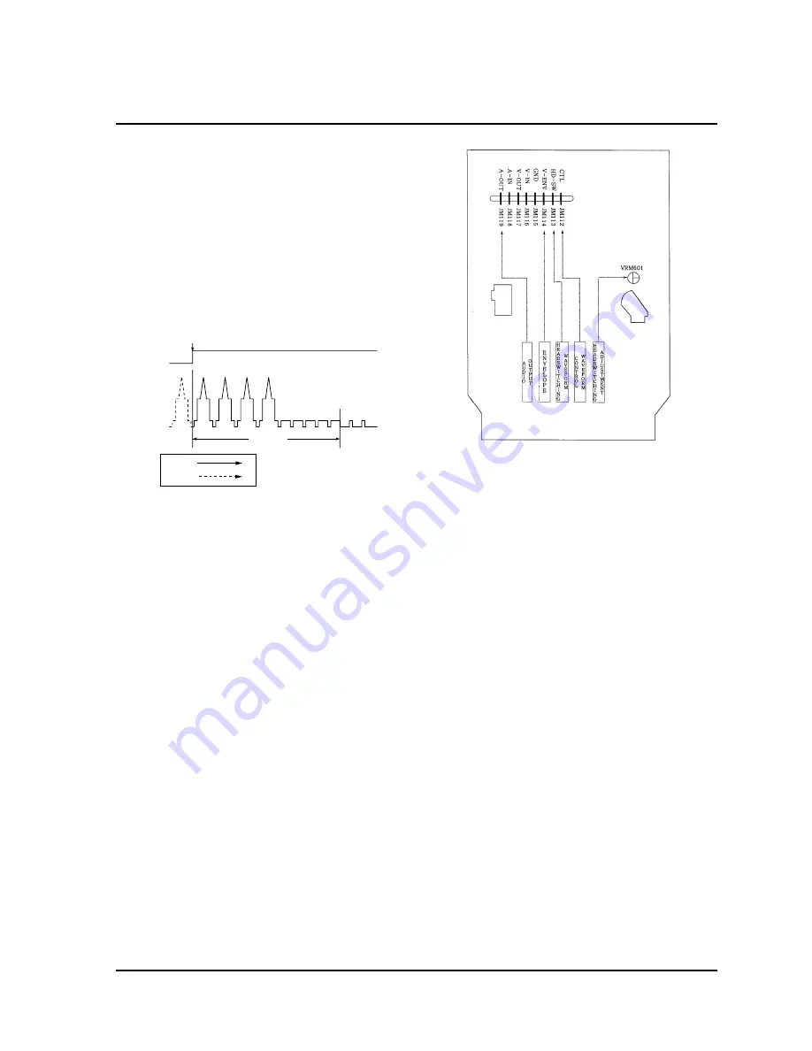
3-5-1 Adjust the switching point.

1. Play back the SP standard tape.

2. Connect the oscilloscope CH1 to EYM03 (HÕD)

and CH2 to EYM11 (V.OUT)

3. Set the oscilloscope sync to CH1, and adjust

VRM601 for 6.5H ± 0.5H waveform as shown
in the figure.

3-5 Circuit (SERVO) Adjustment

6.5H  0.5H

+_

VIDEO

OUTPUT

SWITCHING POINT

SW30Hz
PULSE

Ch2

Ch1

VR
TR

Fig. 3-20

Fig. 3-21

Summary of Contents for TT14A54X/XAX

Page 1: ...54X XAX Television Video Cassette Recorder CONTENTS Precautions Specifications Alignment and Adjustment VCR Alignment and Adjustment TV Timing Chart Troubleshooting Exploded View and Parts List Electric Parts List Block Diagram Wiring Diagram PCB Layout Schematic Diagrams 1 2 3 4 5 6 7 8 9 10 11 12 ...

Page 2: ...ELECTRONICS Samsung Electronics Co Ltd APR 1999 Printed in Korea 3V15A 2001 ...

Page 3: ...s metal cabinets screwheads and control shafts The current measured should not exceed 0 5 milliamp Reverse the power plug prongs in the AC outlet and repeat the test Fig 1 1 AC Leakage Test 6 Antenna Cold Check With the unitÕs AC plug disconnected from the AC source connect an electrical jumper across the two AC prongs Connect one lead of the ohmmeter to an AC prong Connect the other lead to the c...

Page 4: ...appear to have overheated or that are otherwise damaged should be replaced with parts that meet the original specifications Always determine the cause of damage or overheating and correct any potential hazards 15 Observe the original lead dress especially near the following areas Antenna wiring sharp edges and especially the AC and high voltage power supplies Always inspect for pinched out of plac...

Page 5: ...sible conductive parts examples metal panels input terminals and earphone jacks 6 Insulation Checking Procedure Disconnect the power cord from the AC source and turn the power switch ON Connect an insulation resistance meter 500V to the blades of the AC plug The insulation resistance between each blade of the AC plug and accessible conductive parts see above should be greater than 1 megohm 7 Never...

Page 6: ...ctrical charges that damage ESDs 5 Use only a grounded tip soldering iron when soldering or unsoldering ESDs 6 Use only an anti static solder removal device Many solder removal devices are not rated as Òanti staticÓ these can accumulate sufficient electrical charge to damage ESDs 7 Do not remove a replacement ESD from its protective package until you are ready to install it Most replacement ESDs a...

Page 7: ...rack erase 1 audio track erase VIDEO VIDEO Input VIDEO IN jack RCA 1 0Vp p 75 ohm unbalanced Signal to Noise Ratio Better than 35dB Horizontal Resolution Color Monochrome more than 220 lines AUDIO AUDIO Input AUDIO IN jack RCA 8dBm 50kohm unbalanced Horizontal Resolution Color Monochrome more than 220 lines Frequency Response SP 6dB 100Hz 10KHz SLP 6dB 100Hz 5KHz VHF input Ch 2 Ch 13 Cable channel...

Page 8: ...he reference height for the transport adjustment To maintain the height of the tape guide do not apply excessive force onto the main base CYLINDER ASS Y TAKE UP REEL DISK 8 GUIDE POST 9 GUIDE POST SUPPLY REEL DISK CAPSTAN PINCH ROLLER GUIDE ROLLER T GUIDE ROLLER S FULL ERASE HEAD 3 GUIDE POST TENSION POST HEIGHT SCREW TILT SCREW X POSITION ADJUST SILT AZIMUTH SCREW Fig 3 1 Parts Locations of trans...

Page 9: ...head adjustment locations 3 2 2 Adjustments 3 2 2 A A C HEAD HEIGHT ADJUSTMENT 1 Run the alignment tape Color bar in the playback mode 2 Observe surface of the audio head using a dental mirror 3 Turn screw C clockwise or counterclockwise until the gap of lower tape edge and the lower edge of the control head is about 0 25mm Refer to Fig 3 4 and 3 5 Test Points JM112 CTL control waveform JM113 H D ...

Page 10: ...h2 scope probe to JM113 HÕD SW Adjust sync to Channel 1 3 4HD Model Set the control pulse to 6 5 msec using the Fine tracking buttons on the remote control see Fig 3 8 3 9 2HD Model 2 5msec see Fig 3 8 3 9 4 Connect Ch1 scope probe to JM114 ENV 5 Insert the adjusting driver into the X position adjusting gear and adjust the driver for maximum envelope waveform Note Do not adjust the X point using e...

Page 11: ...OVE REMOTE BUTTONS _ _ Fig 3 10 Test Point Position Main PCB Parts Test Points JM113 H D SW head switching sync JM114 EnV envelope waveform 1 Play back the Mono Scope alignment tape SP Mode 2 Observe the video envelope signal on the oscilloscope after taking sync with the video switching pulse 3 Make sure that the video envelope meets the specifications of Fig 3 11 especially for minimum values No...

Page 12: ...e tightness Fig 3 13 Fig 3 12 Adjustment Points A B A B H D SWITCHING PULSE ENVELOPE 7 Play back the Mono Scope alignment tape SP Mode 8 Connect CH1 to JM114 ENV and CH2 to JM113 HÕD for taking sync located on the same PCB 9 Turn the guide roller head with a flat head screw driver to obtain a flat video RF envelope as shown in Fig 3 14 10 After completing the adjustments tighten the set screw Fig ...

Page 13: ... T 120 and T 160 tapes and make sure that the playback output envelope meets the specification show in Fig 3 16 2 Play back a self recorded tape use a T 120 The video envelope should meet the specification shown in Fig 3 16 In SLP Mode A should be the same as B If the head gap is wide check the cylinder 3 2 5 Tape Wrinkle Check 1 Run the T 180 tape in playback FPS RPS and the Pause Modes and obser...

Page 14: ...auses the Holder Clutch AssÕy to rotate through the Belt Pulley 2 The spring wrap PLAY REV of holder clutch assÕy drives the disk reel S T through gear idle by rotation of gear center assÕy 3 Brake is operated by slider cam at FF REW mode 4 Transportation of accurate driving force is done by gears Gear Center AssÕy Note If the spec does not meet the followings specifications replace the holder clu...

Page 15: ...pecting it with Back Tension Meter 1 0mm 0 5mm ˇ LEVER TENSION ASS Y Œ DISK S REEL ADJUSTING ADJUSTING SLIT 1 3 Fig 3 19 Tension Pole and Back Tension Adjustment 1 Remove the holder cassette assÕy and then push the lever FL Arm R to the direction of loading 2 Push the lever tension drive Œ in the direction of arrow See Fig 3 17 3 Turn the gear worm wheel clockwise so that ÒTiming PointÓ of the sli...

Page 16: ...the SP standard tape 2 Connect the oscilloscope CH1 to EYM03 HÕD and CH2 to EYM11 V OUT 3 Set the oscilloscope sync to CH1 and adjust VRM601 for 6 5H 0 5H waveform as shown in the figure 3 5 Circuit SERVO Adjustment 6 5H 0 5H _ VIDEO OUTPUT SWITCHING POINT SW30Hz PULSE Ch2 Ch1 VR TR Fig 3 20 Fig 3 21 ...

Page 17: ... T CARE 0 0 0 1 1 0 0 0 1 0 0 0 0 0 1 1 1 0 0 0 1 0 0 0 1 0 0 1 1 0 1 STAND BY POWER OFF LOADING START LOADING END REV PLAY STOP1 STOP2 FF REV1 FF REV2 0 1 1 1 X X 1 X X X Eject Unload Power Off Tape loading start point Tape loading end point Reverse Picture Search Reverse SLOW Play Rec F PS Still SLOW F ADV Stop Play position 5 Min over MAIN Break ON MODE High speed Rew Low speed FF High speed FF...

Page 18: ...ce F801 Abnormal Normal Abnormal Normal Check secondary power line voltage 5V 6V 16 5V Check the secondary terminal short open of trans Abnormal Abnormal Normal Check the voltage of IC901 pin 34 normal 5V Check the H Sync of pin 26 and the V Sync of pin 27 Check Replace IC901 Check IC901 Pin 17 High when power On Check Replace IC902 Check Replace Q804 Check the voltage of Q804 coil pin Check the v...

Page 19: ... Check the signal output to IC202 Pin 6 Check C239 Check the signal output to IC201 Pin 41 Check the voltage of tuner Check the signal input of IC201 Pin 37 Check Replace IC201 Check the signal output to IC201 Pin 41 Check Replace tuner Check T444 B 125V Check the coil voltage of Q804 Check the signal input to IC200 Pin 19 20 21 Check the voltage IC200 Pin 29 Check the voltage of Tuner Check the v...

Page 20: ... audio signal output from IC201 Pin 54 Check IC901 TV Pin 15 High Line Pin14 High Check IC901 Check the Audio signal input to VCR Check VCR Check the signal input to IC201 Pin 53 55 Check the signal change of IC201 depending on the change of VOL Check Replace IC201 Check IC901 Pin 16 Check Q902 Check the signal input to IC601 Pin 3 Normal Check Replace IC601 Check the VDD input to IC601 Check 13 5...

Page 21: ...place R409 Check IC301 Check the waveform of IC201 Pin 24 Check vertical output terminal circuit Replace IC301 Check IC201 Check Check Replace DY or FBT Normal 6 5 No Color Normal Abnormal Abnormal Abnormal Normal Check the signal input to IC201 Pin 45 Check Q202 IC201 Check IC201 Check IC201 Pin 12 Check C213 X201 Check IC201 ...

Page 22: ...eck the line of RM514 CM515 LM503 RM501 RM502 A out Line Check if ICM301 Pin 16 17 is Low 0 0 5V Replace ICM301 Check the PC 5V of ICM301 Pin 75 Check AC head line and CNM501 Check the PC 5V line Replace ICM301 Check the Audio signal of ICM301 Pin 1 100 Check the A EE PB REC Line and D REC Line ICM601 78 94 Pin Check Abnormal Normal Abnormal Abnormal ...

Page 23: ...Check the REC bias signal of FLM501 Pin 5 6 Over 65Khz 35Vp p Abnormal Check Replace QM504 QM505 Abnormal Normal Normal Check if the QM504 QM505 base voltage is low Check AC head line and CNM501 Check the D REC A EE PB REC terminal line ICM601 78 Pin 94 Replace QM501 Abnormal Normal Check if the QM501 base voltage is high Check the D REC terminal line ICM601 Pin 78 Check the PC 5V line Normal Norm...

Page 24: ...k ICM601 Pin 24 SW 30Hz Check the rotation of capstan Check ICM601 Pin 84 85 Check ICM601 Pin 18 High ICM601 Pin 17 Low Check ICM601 Pin 4 5 6 PROG SW Replace ICM601 Replace ICM601 Normal Normal Abnormal Normal Abnormal Abnormal Refer to Cylinder doesn t rotate Abnormal Check ICM601 Pin 3 8 D FG and Pin 39 D PG Abnormal Refer to Capstan doesn t Rotate Abnormal Check PTM602 PTM601 T Reel takeup sen...

Page 25: ...is high D REC Check ICM601 Check the tape takeout Check the tape Refer to No REC Screen Abnormal Normal Abnormal Check the logic of ICM601 Pin 4 5 6 PROG A B C 6 10 FF Doesn t Operate Normal Stop Normal Insert a tape and operate FF Check ICM601 Pin 4 5 6 PROG SW Check the rotation of capstan Refer to Capstan doesn t rotate Check the Deck Refer to Deck doesn t operate during Playback Abnormal ...

Page 26: ...ion Search Screen Doesn t Operate Searching Speed Normal Check the speed of capstan motor Check if the noise bar is fixed Check the capstan motor Check Replace ICM601 Abnormal Check the B Capstan Motor Playback Speed Set to right direction search screen mode Normal Check the PLAYBACK operation Refer to PLAYBACK Doesn t Operate Abnormal Normal Check the C FG input of ICM601 Pin 88 40 Check the Deck...

Page 27: ...heck the deck Abnormal Check the PLAYBACK operation Refer to PLAYBACK Doesn t Operate Abnormal Normal Search towards right Abnormal Check the C FG input of ICM601 Pin 88 40 Normal Normal Check ICM601 Pin 79 and CAP F R Check for noise bar Check the capstan motor Check Replace ICM601 Abnormal Check the B Capstan Motor Check the control pulse of ICM601 Pin 37 Readjust the height of A C head Abnormal...

Page 28: ...ert a tape Check the followings ICM601 Pin 17 HIGH ICM601 Pin 18 LOW Check the voltage of ICM603 PC 9V Check the B terminal of loading motor Check Replace the loading motor Replace ICM601 Abnormal Normal Abnormal Check of ICM603 Check ICM601 Pin 4 5 6 Replace ICM603 Normal Abnormal ...

Page 29: ...01 Pin 8 5V Check the AL 5V Check the capstan motor Abnormal Abnormal Insert a tape and set to the PLAYBACK mode Normal Check ICM601 Pin 15 22 41 5V Check the AL line 5V Abnormal Check the capstan PWM CTL at ICM601 Pin 25 Replace ICM601 Abnormal Normal Check the input to CNM201 Pin 5 PC 9V Check the PC 9V line HSR 15V Line Abnormal ...

Page 30: ... Insert a tape and set to the PLAYBCAK mode Normal Check the head SW pulse at ICM601 Pin 24 Check the DPG at ICM601 Pin 39 Abnormal Check the PWM at ICM601 Pin 26 Check the voltage of ICM601 Pin 22 15 41 Abnormal Normal Check DFG at ICM601 Pin 38 Check the cylinder motor Abnormal Normal Check the voltage of CNM202 Pin 4 PC 12V Check the motor B line Abnormal Check XTM601 10MHz Normal Normal ...

Page 31: ...the PLAYBCAK mode Check IC201 neighbor circuits Normal Check the video output signal at ICM301 Pin 35 Replace ICM301 Abnormal Normal Check the video signal at ICM301 PIn 25 Check the output of video signal at CM305 Abnormal Check the video signal at ICM301 Pin 28 Replace ICM301 Abnormal Check the voltage of ICM301 Pin 11 16 Low Abnormal Check the voltage of ICM601 pin 78 LOW Normal Normal ...

Page 32: ...e Normal Check the ICM301 Pin 42 has the Video input signal Check the Input Output block IC201 Abnormal Check the ICM301 Pin 66 has the FM video signal Replace ICM301 Abnormal Check the high voltage of ICM301 Pin 16 High Abnormal Check the high voltage of ICM601 Pin 78 D REC Normal Check the video head DRUM Normal ...

Page 33: ...Pin 72 has the color signal Check Pin 14 Rotary Check ICM301 62 OSC 3 57MHz 30Hz Replace ICM301 XTM301 Replace Check the ICM301 Pin 74 has the ENVE Signal Normal DRUM Check Check the voltage of ICM301 Pin 16 Low Check the voltage of ICM601 Pin 78 D REC Abnormal Abnormal Normal Normal Normal Abnormal Abnormal _ ...

Page 34: ...ormal Normal No Color On REC Check the ICM301 Pin 72 has the color signal Check ICM301 62 OSC 3 5795MHz 30Hz Replace XTM301 Check the color signal of ICM301 Pin 66 Replace ICM301 Check connecting pattern and Pin 14 Rorary SW Replace ICM301 Abnormal Normal Normal Abnormal _ ...

Page 35: ...704 000103 SOCKET CRT 10P 22 5PI 14 3PI S 1 V999 3 AA64 00055B CABINET BACK TT14A5 HIPS HB BLK 1 3 1 6002 000514 SCREW TAPPING RH 2 M4 L15 ZP 6 CB CF 3 2 L9400 0002 ANT RODVHF 4SDODIPOLE500MMBRN 1 4 AA61 20070A POWERCORDEP2N P L3000 0001 2 1 1 A AA94 10149X ASSY PCB MAIN OPT V15A 14 S V MEXICO 1 A 1 AA60 10008A SCREW TAPPING TH M3 L10 ZP 7 PCB HC A 2 AA61 20231A HOLDER CHASSIS DP AA61 2 1 A 3 AA63...

Page 36: ... CRT CF 2 3 3704 001105 SOCKET CRT 11P 20PI 26 5PI NI 1 V999 3 AA64 00056B CABINET BACK TT20A5 HIPS HB BLK 1 3 1 6002 000514 SCREW TAPPING RH 2 M4 L15 ZP 6 CB CF 3 2 L7000 0130 ANT RODVHF 4SDODIPOLE500MMBRN 1 4 L3000 0001 POWER CORD AC DW 006 MSP 10 SPC 2 2100 1 A AA94 10149W ASSY PCB MAIN OPT V15A 19 S V MEXICO 1 A 1 AA60 10008A SCREW TAPPING TH M3 L10 ZP 6 PCB HC A 2 AA61 20232A HOLDER CHASSIS D...

Page 37: ... G450 AC66 80141A SLIDER TAKE UP ASSY X 9 TS X 9 G480 AC33 10217H HEAD ACE ASSY X 9 G510 AC60 10518A SCREW TAP TITE PH SW ZW M2 6 L5 6 ZP G520 AC66 30539A LEVER 9 GUIDE ASSY X 9 TS X 9 G527 AC61 60553A SPRING 9 GUIDE ES SUS304 WPB OD3 1 0 G530 AC33 10217G HEAD FE VAA00000275 X 9 G532 AC60 10519A SCREW TAP TITE PH M2 6 L8 ZPC G546 AC66 30535A LEVER FL DOOR POM M90 44 BLK X 9 G555 AC59 90403A UNIT P...

Page 38: ...458 AC66 20574A GEAR JOINT 2 POM SW 01 M1 0 Z14 PCD1 B462 AC60 10517A SCREW TAP TITE PH M2 6 L5 ZPC YE B484 AC66 20580A GEAR LOADING DRIVE POM SW 01 M1 0 Z32 B488 AC66 30543A LEVER S LOAD ASSY X 9 B500 AC66 30542A LEVER T LOAD ASSY X 9 B560 AC31 12017A MOTOR CAPSTAN DMVCMC07C X 9 B570 AC60 10514A SCREW CAPSTAN PH M2 6 L6 G542 AC66 60051A BELT PULLEY 5CM 70 2 2 71 3 X 9 K200 AC61 21012A HOLDER CLUT...

Page 39: ...PS HB BLK BADGE AA64 70009DBADGE BRAND AL L40 GOLD R BOSS L3113 0003 000BOSS CABINET HIPSHBBLK CDCOIL L9400 0002HOLDER DEGAUSSING 20POLYVINI CP AA64 20060DCONTROL PANEL HIPS HB BLK PA100 TT14A5 D COIL AA27 20004CCOIL DEGAUSSING 14 4 5ohm 30T L890 D F C AA64 00123ALASSY FRONT HIPS HB BLK PA100 TT14A5 F C AA64 00123BCABINET FRONT HIPS HB BLK PA100 TT14A5 ASSY SPEAKER AA96 40056AASSY SPEAKER 8OHM 2W ...

Page 40: ...MIC DISC 10NF 80 20 50 C304 2401 000553 C AL 1UF 10 50V GP 5X11MM 5MM C305 2305 000427 C FILM MPEF 47NF 5 100V 7 5X1 C306 2401 000173 C AL 1000uF 20 35V GP TP 13x25 5 C308 2301 000310 C FILM PEF 68NF 5 50V 8 0X8 5 C309 2401 000360 C AL 100UF 20 50V GP 8X11MM 5 C310 2401 000493 C AL 10UF 20 50V WT 5X11MM 5M C311 2401 001333 C ELECTROLYTIC CE04WTAPG50V0 4 C312 2401 000553 C AL 1UF 10 50V GP 5X11MM 5...

Page 41: ... 0402 000132 DIODE RECTIFIER 1N4004 400V 1A DO 41 D817 0402 000132 DIODE RECTIFIER 1N4004 400V 1A DO 41 D901 0403 000355 DIODEZENER UZ5 1BSB 4 97 5 17V 0 5UA 500 D903 0401 000005 DIODE 1N4148TAPG D904 0401 000005 DIODE 1N4148TAPG DX01 0403 000297 DIODE ZENER EQA02 06D MTZ6 2B DX02 0402 000132 DIODE RECTIFIER 1N4004 400V 1A DO 41 DZ801 1405 001036 VARISTOR 430V 2500A 14x8 5mm TP DZ802 0403 000300 D...

Page 42: ... R METAL OXIDE S 7 5KOHM 5 2W AF TP 3 7 R416 2001 000022 R CARBON S 33OHM 5 1 2W AA T R444 2001 000109 R CARBON S 470OHM 5 1 2W AA R501 2001 000007 R CARBON 3KOHM 5 1 8W AA TP 1 R502 2001 000007 R CARBON 3KOHM 5 1 8W AA TP 1 R503 2001 000007 R CARBON 3KOHM 5 1 8W AA TP 1 R504 2003 000784 R METAL OXIDE S 7 5KOHM 5 2W AF TP 3 7 R504A 2003 000784 R METAL OXIDE S 7 5KOHM 5 2W AF TP 3 7 R505 2003 00078...

Page 43: ... FERRITEBEAD AA 3 5X1 0X6 BDM603 3301 000287 CORE FERRITEBEAD AA 3 5X1 0X6 CFT FD 6002 000507 SCREW TAPPING RH 2 M3 L12 ZP CM102 2401 002619 C AL 47uF 20 25V GP TP 5x11 5 CM103 2401 000480 C AL 10UF 20 50V GP 5X11MM 5M CM105 2202 002037 C CERAMIC MLC AXIAL 100NF 80 20 CM106 2401 000553 C AL 1UF 10 50V GP 5X11MM 5MM CM107 2401 000553 C AL 1UF 10 50V GP 5X11MM 5MM CM110 2401 002619 C AL 47uF 20 25V ...

Page 44: ...4004 400V 1A DO 41 DM105 0402 000132 DIODE RECTIFIER 1N4004 400V 1A DO 41 DM106 0401 000005 DIODE 1N4148TAPG DM301 0401 000005 DIODE 1N4148TAPG DM302 0401 000005 DIODE 1N4148TAPG DM610 0402 000132 DIODE RECTIFIER 1N4004 400V 1A DO 41 DM611 0401 000005 DIODE 1N4148TAPG DM612 0402 000132 DIODE RECTIFIER 1N4004 400V 1A DO 41 DM613 0402 000132 DIODE RECTIFIER 1N4004 400V 1A DO 41 DM614 0402 000132 DIO...

Page 45: ...P RM618 2004 001185 R METAL 680KOHM 5 1 8W AA TP RM621 2001 000429 R CARBON 1Kohm 5 1 8W AA TP 1 8x3 2mm RM623 2001 000290 R CARBON 10KOHM 5 1 8W AA TP RM633 2001 000429 R CARBON 1Kohm 5 1 8W AA TP 1 8x3 2mm RM634 2001 000429 R CARBON 1Kohm 5 1 8W AA TP 1 8x3 2mm RM636 2001 000429 R CARBON 1Kohm 5 1 8W AA TP 1 8x3 2mm RM638 2001 000734 R CARBON 4 7KOHM 5 1 8W AA TP RM639 2001 000429 R CARBON 1Kohm...

Page 46: ...HM 5 1 2W AA T ASSY ACCESSORY AA97 20032FASSY ACCESSORY V15A MEX TVI TVCR A ROD L7000 0130 ANT RODVHF 4SDODIPOLE500MMBRN BATT 4301 000121 BATTERY MN 1 5V AAA 10 5X44 CR MUL 31499 009 120CR MULTIPLE MED C271 R1 2M I B AA68 00010AMANUAL USERS V15A SPA TM46 W P100 G PATCH AA39 40001F CABLE RCA RCA 150MM 0 12 10 T MATC L2759 115 050TRANS MATCHING R300 R75CSA T REG L6000 0082 020TARJETADEREGISTRO 8 5X1...

Page 47: ... TUNER EXT AUDIO SPEAKER CRT MICOM E2PROM M DECK EXT VIDIO S W IC SPS CONTROL I CHIP SWITCHING TRANS SOUND AMP IC601 CRT DRIVE Q401 H OUT VERTICAL KA2131 5V 6V RF VIDEO AUDIO RF AUDIO 9V RF LINE VIDEO IF SIGNAL SAW I2C BUS CONTROL SF101 12V RGB 24V FBT DY H V ...

Page 48: ...816 199 116 D817 139 94 D818 139 101 D901 139 136 D903 99 87 D904 105 159 DS801 232 106 DS802 233 119 DS803 229 119 DS804 209 126 DS805 232 165 DS806 212 134 DX01 144 115 DX02 128 113 DZ801 212 41 DZ802 185 29 DZ803 194 12 DZ804 193 9 DZ805 119 34 IC201 25 157 IC202 24 199 IC203 33 207 IC301 53 116 IC601 204 176 IC801 171 9 IC802 155 107 IC803 178 156 IC804 117 101 IC901 150 183 IC902 141 153 IC90...

Page 49: ...174 217 DM620 138 49 DM622 172 31 DM701 36 71 ICM101 271 219 ICM102 290 224 ICM301 183 112 ICM601 90 56 ICM603 53 211 ICM605 138 45 QM101 191 44 QM102 201 44 QM103 164 44 QM104 177 44 QM106 210 231 QM301 224 174 QM302 246 170 QM303 174 147 QM304 145 120 QM305 197 65 QM306 270 108 QM307 146 203 QM308 270 150 QM501 252 100 QM502 242 90 QM503 252 84 QM504 252 106 QM505 252 110 QM601 133 56 QM602 141 ...

Page 50: ...PCB Layout Samsung Electronics 11 3 11 3 Main CONTROL ...

Page 51: ...10 Wiring Diagram Wiring Diagram Samsung Electronics 10 1 ...

Page 52: ...H e e e h f e f e f W Y e V4 6X TP1 e W2 6Xe e e O2 W2 6X W2 6X W2 6X f W2 6Xe O2 g eO2 heO2 e W2 6X f W2 6X 7 eB1e L e e 7 1 7 e 1 7 1 fJ 5 7 e 1e gJ 5 hf f 7 MI 1 f f 7 1 e e W2 6Xe 6X e 6Xe W2 Le e 5 e f7 H e f g7 H e f Y e f f 3 f N fW 1e 1 e e 1eW V K H e e J 5e e f f J 5f 6X he 6X gW 5 6Xf 6X 3 5 V4 6X e e W 5e eJ 5 J 5e W M 3 3 e 3 e 7 He e f f 7 Hf 0MI 1 he 0MI 1 f W Y 0MI 1f 0MI 1e 1 J 5e...

Page 53: ... h e e e f e e O K e he f h O Kf g W K e h e e e e e f 5 g hf e W J f h X W e Hh h W2 e f he g X I X g hf he f e 7 6Xe W2 6X g O2 eW2 6XgO2 7 6T5 W2 g O2 eW2 6XgO e e f hW Y J 6Xg g g g h V X I X W MI Xe g e7 e 1 I U W MI he e7 e 1 h7 H f7 e 1 J 5g heN 1 eN 1 7 H V4 e h e e e eN 1 7 H V4 he e e e h e f e 6T2 6X W2 6Xf 7 HeW2 f e e e e e g e e e g h e 6X e 1 7 I4 fJ 5 W M 3 L J 5 e e e e g e g he e...

Page 54: ...Schematic Diagrams 12 3 Samsung Electronics 12 3 VCR POWER BLOCK ...

Page 55: ...hematic Diagrams 12 4 Samsung Electronics 12 4 TV MAIN BLOCK TP17 TP18 TP19 TP11 TP12 TP13 TP15 TP16 TP14 TP27 TP28 TP29 TP30 TP32 TP31 TP35 TP25 TP26 TP24 TP23 TP21 TP22 TP20 TP36 Power Line Signal Line ...

Page 56: ...Schematic Diagrams 12 5 Samsung Electronics TP11 TP12 TP13 TP14 TP15 TP16 TP17 TP18 TP19 TP20 TP21 TP22 TP23 TP24 TP25 TP26 TP27 TP28 TP29 TP35 TP36 TP30 TP31 TP32 TP33 TP34 12 4 1 Waveform ...

Reviews: