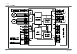
Block Diagrams
9-2
Samsung Electronics
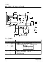
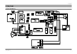
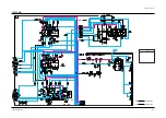
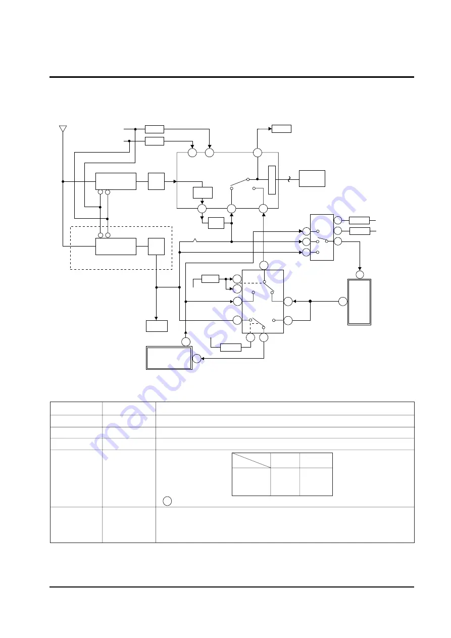
9-2 C15A Video Block Diagram (Continued)
MICOM#24
ANT
MICOM #23
SDA
SCL
1st
IF
1st Tunning
7
8
IF
DET.
2nd Tunning
2nd
IF
Trap
6
13
17
1T.option
#13
VPS
ICP01
CN101 PB.V
2
PB H
11
10
1
5
Micom #6
Micom #8
Module
DECK
4
CN101
REC. SOURCE V.
AV/Tuner
9
4
H
L
2
3
15
IC701
V-out
V-in
VCR
or
Decorder
PB H
V/T/H
Micom #6
Micom #7
IC702
2
1
5
9
10
3
IC201
INT
EXT
R
G
B
38
CRT
Drive
TTX
#8
ICT01
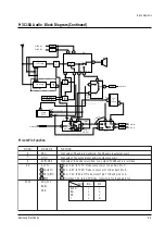
C15A OPTION
Micom Pin Function
PIN NO.
6
7
8
56, 57
23,24
PIN NAME
PB H
V/T/H
AV/TUNER
S-L H
FRA H
SDA,SCL
FUNCTION
High Output : Playback signal is monitored. The PB signal is output at scart.
High Output : The second tuner signal is output at scart.
High Output : AV signal is recorded. Low output : TUNER signal is recorded.
a C. SYSTEM : PAL/SEC ARE AUTO mode, and France is SECAM mode.
Extra control signals are all controlled by the I
2
C bus.
Select INT/EXT
FRENCH system modulation
Port
S
PAL/SEC
FRANCE-L
FRANCE-L'
FRA H
L
H
L
S-L H
L
L
H
Summary of Contents for TW14C52S/BWT
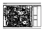
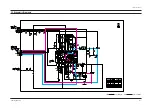
Page 89: ...11 Wiring Diagram 11 1 C15A Wiring Diagram Wiring Diagram Samsung Electronics 11 1 ...
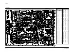
Page 90: ...Wiring Diagram 11 2 Samsung Electronics 11 2 C15A Wiring Diagram ...
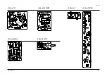
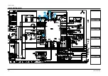
Page 94: ...Schematic Diagrams 12 4 Samsung Electronics 12 4 VCR POWER BLOCK ...
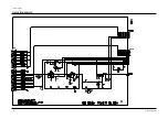
Page 97: ...Schematic Diagrams 12 7 Samsung Electronics 12 7 TV 3 4 RED POWER LINE BLUE SIGNAL LINE ...

