10-14
Samsung Electronics
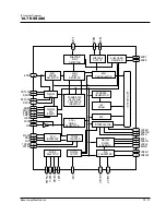
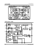
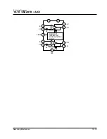
IC Internal Diagram
No. 5688-2/9
LA1837
Parameter
Symbol
Conditions
Ratings
Unit
min
typ
max
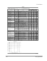
[FM Mono Characteristics] fc = 10.7 MHz, fm = 1 kHz, with the coil adjusted so that V
AFC
– V
REG
= 0 V
Current drain
I
CCO
-FM
With no input
18
31
44
mA
Demodulation output
V
O
FM
100 dBµ, 100% mod. The pin 16 output
730
1100
1460
mVrms
Channel balance
C.B-mono
100 dBµ, 100% mod. The pin 16 output/pin 17 output
–1.5
0
+1.5
dB
Total harmonic distortion (mono)
THD
FM(1)
100 dBµ, 100% mod. The pin 16 output
0.3
1.3
%
Total harmonic distortion (mono)
THD
FM(2)
100 dBµ, 200% mod. The pin 16 output
1.0
5
%
Signal-to-noise ratio
S/N
FM
100 dBµ, 100% mod. The pin 16 output
72
80
dB
AM rejection ratio
AMR
100 dBµ, AM 30 % mod. The pin 16 output
45
65
dB
Limiting input voltage
–3 dBL.S.
100 dBµ, 100% mod. Referenced to the output.
26
32
38
dBµ
The input such that the output is down –3 dB.
LED sensitivity
SD
On-FM
51
60
69
dBµ
LED bandwidth
SD
BW
100 dBµ
85
120
170
kHz
IF count buffer output
V
IFBuff-FM
100 dBµ. The pin 13 output
80
120
160
mVrms
S-meter output
V
SM-FM(1)
0 dBµ. The pin 11 output
0
0.1
0.5
V
V
SM-FM(2)
100 dBµ. The pin 11 output
3.6
4.3
5.0
V
Muting attenuation
Mute-Att
100 dBµ, 100% mod. The pin 16 output
75
85
dB
[FM Stereo Characteristics] fc = 10.7 MHz, 100 dBµ, fm = 1 kHz, L + R = 90%, Pilot = 10%
Separation (left)
Sep
L
L mod. The pin 16 output/pin 17 output
30
45
dB
Separation (right)
Sep
R
R mod. The pin 17 output/pin 16 output
30
45
dB
Stereo on level
ST
ON
The pilot modulation such that V7 is under 0.7 V.
1.3
2.7
5
%
Stereo off level
ST
OFF
The pilot modulation such that V7 is over 4.5 V.
1.5
%
Total harmonic distortion (main)
THD-main
L+R mod. The pin 16 output
0.3
1.3
%
Brej-3rd
fs = 113 kHz, Vs = 90 %, Pilot = 10 %, The pin
40
dB
Adjacent channel interference
16 output vs. the L-R mod. 1 kHz demodulated output
rejection ratio
Brej-5th
fs = 189 kHz, Vs = 90 %, Pilot = 10 %, The pin
40
dB
16 output vs. the L-R mod. 1 kHz demodulated output
[AM Characteristics] fc = 1000 kHz, fm = 1 kHz
Current drain
I
CCO-AM
With no input
15
25
35
mA
Detector output
V
OAM(1)
23 dBµ, 30% mod. The pin 16 output
100
180
360
mVrms
V
OAM(2)
80 dBµ, 30% mod. The pin 16 output
200
320
500
mVrms
Signal-to-noise ratio
S/N
AM(1)
23 dBµ, 30% mod. The pin 16 output
18
22
dB
S/N
AM(2)
80 dBµ, 30% mod. The pin 16 output
49
55
dB
Total harmonic distortion (mono)
THD
AM(1)
80 dBµ, 30% mod. The pin 16 output
0.4
1.2
%
THD
AM(2)
80 dBµ, 80% mod. The pin 16 output
1.0
4.0
%
LED sensitivity
SD
On-AM
17
27
37
dBµ
Local oscillator buffer output
V
OSC-AM
With no input. The pin 30 output
110
160
220
mVrms
IF counter buffer output
V
IFBuff-AM
80 dBµ, no modulation. The pin 13 output
160
220
300
mVrms
ST-IF output
V
STIF-AM
80 dBµ, no modulation. The pin 7 output
16
34
48
mVrms
S-meter output
V
SM-AM
0 dBµ, no modulation.
0
0
0.2
V
Electrical Characteristics
at Ta = 25°C, V
CC
= 9 V, in the specified Test Circuit
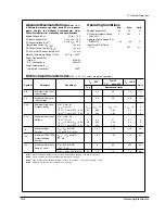
Allowable power dissipation, Pd max
–
mW
Ambient temperature, Ta – °C
Pd max – Ta
Summary of Contents for Wingo S-2450
Page 2: ...ELECTRONICS Samsung Electronics Co Ltd SEP 2000 Printed in Korea Code no AH68 00036D ...
Page 14: ...Samsung Electronics 5 1 5 Block Diagram 5 1 Main ...
Page 17: ...6 2 Samsung Electronics 6 4 Jack PCB 6 5 Motor PCB 6 6 POWER S 2400 2450 ...
Page 18: ...Samsung Electronics 6 3 6 7 MAIN ...
Page 19: ...6 4 Samsung Electronics 6 8 CD 6 9 MP3 Charge MP3 Jack ...
Page 20: ...Samsung Electronics 6 5 6 10 Adapter Batt Sense 6 11 ENCODER ...
Page 21: ...ENCODER PCB DIAGRAM only S2450 Model ...
Page 22: ...ENCODER PCB DIAGRAM only S2450 Model ...
Page 23: ...Samsung Electronics 7 1 7 Wiring Diagram Optical Output Option NCW100 ...
Page 24: ...Samsung Electronics 8 1 8 Schematic Diagram 8 1 Main Part ...
Page 25: ...8 2 Samsung Electronics 8 2 CD ...
Page 26: ...Samsung Electronics 8 3 8 3 ENCODER ...
Page 27: ...ENCODER SCHEMATIC DIAGRAM only S2450 Model ...
Page 28: ...ENCODER SCHEMATIC DIAGRAM only S2450 Model ...
Page 41: ...Samsung Electronics 10 5 IC Internal Diagram Audio ICs BA3121 BA3121F BA3121N FBlock diagrams ...
Page 47: ...Samsung Electronics 10 11 IC Internal Diagram Audio ICs BU1923 BU1923F FBlock diagram ...
Page 56: ...10 20 Samsung Electronics IC Internal Diagram 10 11 TDA7440D JIC1 ...

