background image

WSM520V


Version 1.0 

Samsung Electronics 

page 4 of 8


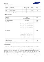
5. Operating Conditions 


Symbol Parameter 

Min. Typ. Max. 

Unit 

V dc 

Supply Voltage 

4.5 

5.0 

5.5 

I dc 

Supply current 

500 

mA 

Temp Operating 

Temperature 

5    35 


6. RF Characteristics 


Parameter Value 

Unit 

Modulation 

Pi/4DQPSK


/ SSB 


RF Frequency Range 

5725 – 5825 

MHz 

Bandwidth 2 

MHz 

RF Frequency  

Channel (0)   LO : 5725,  Fc: 

NOT USED 

Channel (1)   LO : 5727,  Fc: 

NOT USED 

Channel (2)   LO : 5729,  Fc: 5730.35 
Channel (3)   LO : 5731,  Fc: 5732.35


Channel (4)   LO : 5733,  Fc: 5734.35


Channel (45)  LO : 5815,  Fc: 5816.35


Channel (46)  LO : 5817,  Fc: 5818.35


Channel (47)  LO : 5819,  Fc: 5820.35


Channel (48)  LO : 5821,  Fc: 

NOT USED 

Channel (49)  LO : 5823,  Fc: 

NOT USED 

MHz 

Diversity 

1TX / 2RX 


Antenna peak gain 

2.2 

dBi 

RF TX output power (tolerance) 

14.0 (+2dB) 

dBm 


7. Transmit mode 


 In transmit mode, the audio engine transforms the audio data into packetized digital IQ signals. These 

are in turn pulse-shaped before conversion by DAC to match to the analog IQ inputs of the radio 

transceiver. The radio transceiver has programmable baseband filter to lower the RF spectrum side lobes 

and to suppress the DAC image and the DAC spurious. The output power is programmable. A power 

detector (PD_Out) on the radio transceiver enables close-loop TX power control.  The differential RF TX 

DA outputs are connected via a balun filter to Power amplifier and the amplified TX carrier signal is 

radiated by a printed antenna in the module after going through Transmit/Receive switch placed between 

Summary of Contents for WSM520V

Page 1: ...he necessary radio transceiver and digital baseband circuitry to form a complete digital wireless node without the need for external processing The WSM520V can be powered from a 5V supply input and the AV5100 contains all the necessary power management and analog circuitry needed to operate the chip The WSM520V can operate in upper bands 5725 5825MHz of 5GHz spectrum enabling worldwide coverage 2 ...

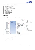
Page 2: ...uration Low fixed latency 20ms Separate RF transmit and receive RF I O RX diversity USB digital audio capability I2S digital audio capability Complete power management 24pin I O connector 3 Block Diagram The Block diagram of WSM520V module is shown in the below picture WSM520V block diagram PCB Antenna 0 5725 5825MHz PCB Antenna 1 5725 5825MHz X TAL 16MHz ...

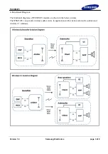
Page 3: ...onics page 3 of 8 4 Functional Diagram The functional diagrams of WSM520V module are shown in the below pictures The WSM520V can provide wireless audio service in applications with wireless subwoofer solution and wireless 2 1 solutions ...

Page 4: ...23 Fc NOT USED MHz Diversity 1TX 2RX Antenna peak gain 2 2 dBi RF TX output power tolerance 14 0 2dB dBm 7 Transmit mode In transmit mode the audio engine transforms the audio data into packetized digital IQ signals These are in turn pulse shaped before conversion by DAC to match to the analog IQ inputs of the radio transceiver The radio transceiver has programmable baseband filter to lower the RF...

Page 5: ...or is configured as the following table Pin Number Pin Name I O Description 1 VDD_5V PWR Regulated 4 5V to 5 5V input 2 VDD_5V PWR Regulated 4 5V to 5 5V input 3 GPIO5 I2CS_SCL I O I2C serial clock slave 4 GPIO4 I2CS_SDA I O I2C serial data slave 5 GPIO19 WCLK1 I O I2S Left Light clock 1 6 RESET I Reset 7 GPIO9 MISO_EXT_FLASH I O External flash memory data output 8 GPIO8 MOSI_EXT_FLASH I O Externa...

Page 6: ...ll not occur in a particular installation If this equipment does cause harmful interference to radio or television reception which can be determined by turning the equipment off and on the user is encouraged to try to correct the interference by one or more of the following measures Reorient or relocate the receiving antenna Increase the separation between the equipment and receiver Connect the eq...

Page 7: ...rmful interference and 2 this device must accept any interference received including interference that may cause undesired operation This Class B digital apparatus complies with Canadian ICES 003 Operation is subject to the following two conditions 3 this device may not cause harmful interference and 4 this device must accept any interference received including interference that may cause undesire...

Page 8: ...t the end user has to be informed to keep at least 20cm separation with the antenna while this end product is installed and operated The end user has to be informed that the IC radio frequency exposure guidelines for an uncontrolled environment can be satisfied The end user has to also be informed that any changes or modifications not expressly approved by the manufacturer could void the user s au...

Reviews: