background image

4-16

Samsung Electronics

Troubleshooting

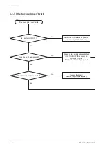
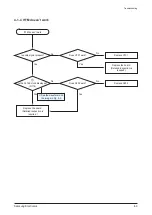
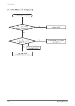
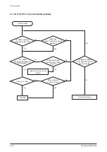
4-1-7  If the MIC doesn’t work properly

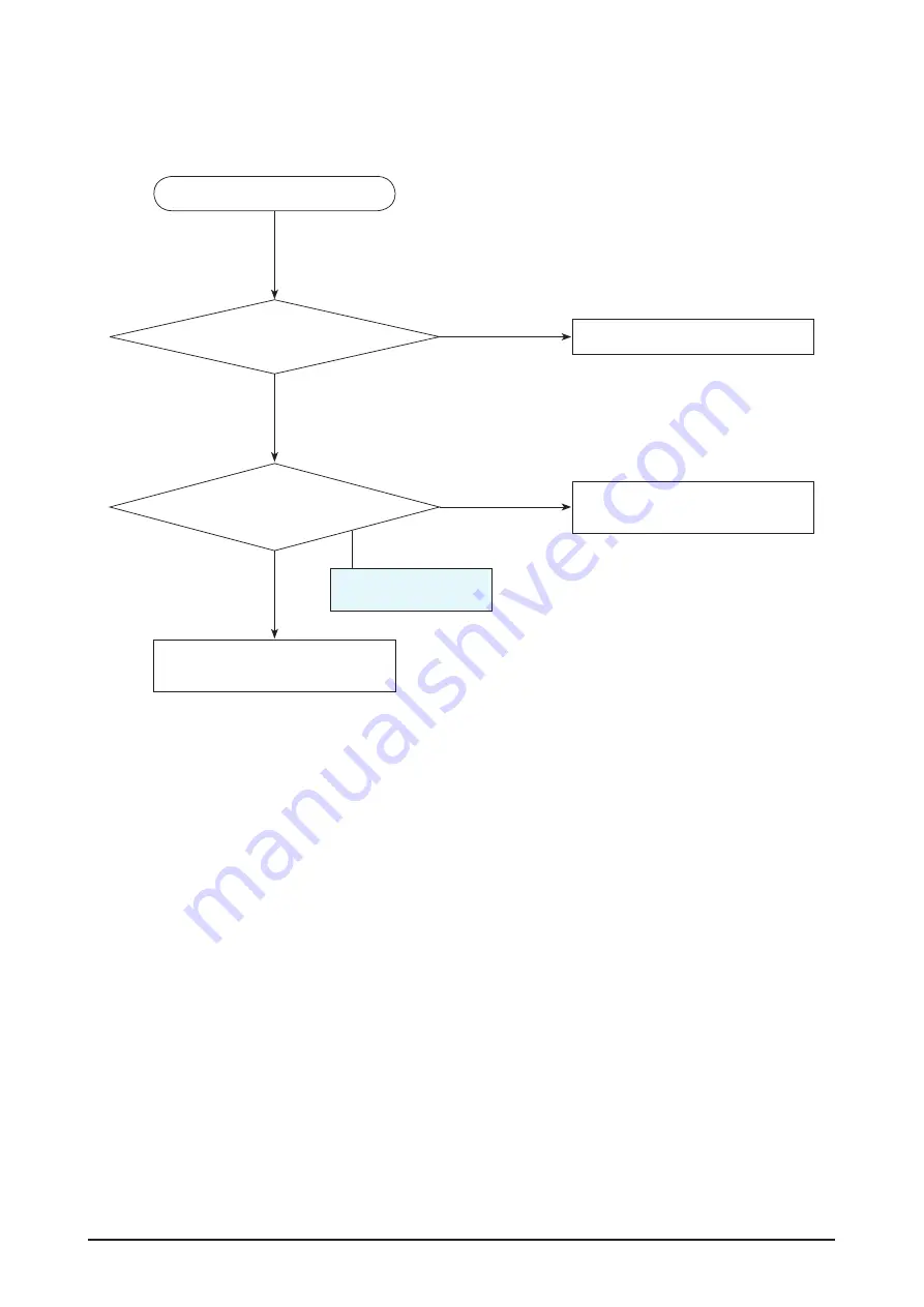
1

Is the bias voltage present?

(R704 - 1.5V)

Does the MIC look fine  

when checking visually?

Replace the MIC.

Disassemble the main body and 

replace the MIC.

Replace the board. 

(Detailed inspection is required.)

Yes

No

Yes

No

If the MIC doesn’t work properly

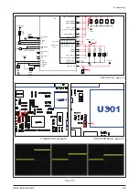
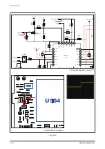
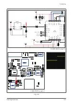
 See the waveform and 

the image in Fig. 4-9.

Summary of Contents for YP-R1

Page 1: ...MP3 Player Model Name YP R1 Model Code YP R1AB XER MP3 Player CONTENTS 1 Precaution 2 Product Specification 3 Disassembly Reassembly 4 Troubleshooting 5 Exploded View Part List 6 PCB Diagram 7 Schematic Diagram YP R1 ...

Page 2: ...r domestic law GSPN Global Service Partner Network Area Web Site North America service samsungportal com Latin America latin samsungportal com CIS cis samsungportal com Europe europe samsungportal com China china samsungportal com Asia asia samsungportal com Mideast Africa mea samsungportal com Samsung Electronics Co Ltd Oct 2009 Printed in Korea ...

Page 3: ...assembly 3 1 4 Troubleshooting 4 1 Checkpoints by Error Mode 4 1 4 2 Upgrade Methods 4 23 5 Exploded View Part List 5 1 Exploded View 5 1 5 2 Electrical Part List 5 3 6 PCB Diagram 6 1 MAIN PCB Top 6 1 6 2 MAIN PCB Bottom 6 3 7 Schematic Diagram 7 1 Overall Block Diagram 7 1 7 2 MAIN CPU 1 7 2 7 3 MAIN CPU 2 7 3 7 4 Memory SDRAM NAND Flash 7 4 7 5 Power Management 7 5 7 6 AUDIO CODEC 7 6 7 7 24PIN...

Page 4: ...ld not use any attachments that are not recommended by the company This could cause damage to the unit 3 You should not use this product near or in water 4 You should only use the power supply provided by the company 5 If replacement material is required you should only use standardized materials if you use non standardized materials you could cause failure to the product ...

Page 5: ... electrostatic charge 4 Do not use freon propelled chemicals These can generate electrical charges that damage ESDs 5 Use only a grounded tip soldering iron when soldering or unsoldering ESDs 6 Use only an anti static solder removal device Many solder removal devices are not rated as anti static these can accumulate sufficient electrical charge to damage ESDs 7 Do not remove a replacement ESD from...

Page 6: ...ntuitive menu selection that you can navigate with your fingertips on a full screen touch pad Video playback without converting Playback is possible by simply transferring files without converting All file formats to the right are supported Compact design Compact design giving excellent portability 45 5 H x 85 2 V x 8 9 D mm ...

Page 7: ...dvanced Profile level1 10 Mbps WMA MP4 MPEG4 Max 720 X 480 Advanced Simple Profile Level 5 8 Mbps H 264 AVC Max 720 X 480 High Profile Level3 0 12 5 Mbps MP3 AAC AAC WMV ASF WMV9 MAX 720 X 480 Advanced Profile level1 vc1 10 Mbps WMA MOV MPEG4 Max 720 X 480 Advanced Simple Profile Level 5 8 Mbps H 264 AVC Max 720 X 480 High Profile Level3 0 12 5 Mbps AAC AAC Image JPEG Baseline Progressive BMP MAX3...

Page 8: ...m FM FM T H D 1 FM Signal to Noise Ratio 55dB FM Useable Sensitivity 38dBμ Wireless System Bluetooth QD ID B015440 Emission Type F1D RF power CLASS I Transmit Frequency 2402MHz 2480MHz Receive Frequency 2402MHz 2480MHz Number of channels 79 channels Modulation System GFSK Communication Mode Semi duplex Operation Humidity 0 95 Specifications Version Supported 2 0 EDR Module BCM2070 ...

Page 9: ...580mAh Playback Time Earphone 25 Hours of Music Playback with Earphones Based on MP3 128 kbps Volume 15 Normal EQ LCD OFF 5 Hours of Video Playback Based on MPEG4 SP Volume 15 Normal EQ LCD lv3 50 Hours of Music Playback with Earphones 4Hours of Video Playback Color Black Silver Pink White Black Blue Capacity 8G 16G 32G 4G 8G 16G CASE Tempered glass Aluminum Plastic ABS Aluminum Plastic NO Convers...

Page 10: ...ry X Playlist DNSE X Speed Control MP3 file play 0 75 1 3X MP3 file play 0 75 1 3X Output Power Earphone 20mW CH 20mW CH TUNER FM RDS X ETC X X FUNCTIONS Alarm X X Bluetooth X Photo Viewer Text Viewer Game Wallpaper World Clock Voice Recording FM Recording X Wise Volume Hearing Protection X Address Book X Data Cast X Flash Player X Calculator X X TTS Text to Speech X FW will be supported X Calende...

Page 11: ...sung Electronics Product Specification 2 4 Accessories 2 4 1 Supplied Accessories Accessories Item Item Code Remark Earphones GM59 01016A Samsung Service Center USB Cable GM39 01002A User s Manual GM68 01002J ...

Page 12: ...rforming any work on the IC chips on the PCB To assemble follow the below instructions in reverse order No Description Description Photo 1 1 Insert a flat screwdriver or tweezers into the hole shown on the right Remove the cover attached with double sided tape Be careful not to make any scratches as you remove the cover 2 1 Remove the two screws using a phillips screwdriver and remove the SUS BRAC...

Page 13: ...CB 6 1 Disconnect the three connectors on the MAIN PCB and remove the FPCB and the MAIN PCB 7 1 Insert a flat screwdriver or tweezers into the hole next to the battery FPCB and remove the battery FPCB 8 1 Remove the battery that is fixed with double sided tape onto the LCD MODULE Ensure that the battery doesn t get damaged ...

Page 14: ...lectronics 3 3 Disassembly Reassembly No Description Description Photo 9 1 When removing the hooked LCD pull the bottom of the LCD 2 upwards while widening the side of the Touch Assy 1 10 1 After disassembly 1 2 ...

Page 15: ...3 4 Samsung Electronics MEMO ...

Page 16: ...o power Check that the firmware is upgraded See 4 2 Upgrade Methods Charge the battery and check that the power is on Yes No 1 2 3 C316 2 5V C318 1 2V C303 3 0V Check the voltage No No No 6 7 Check CPU_RST HIGH R406 LOW 4 5 Check that the clock on X403 and X402 oscillates No Faulty Yes Yes Yes Yes If there is no power See the waveform and the image in Fig 4 1 A B See the waveform and the image in ...

Page 17: ...4 2 Samsung Electronics Troubleshooting Replace the battery and check the voltage again No Complete A B Check the voltage on the battery ...

Page 18: ... VREFIN P11 VREOUT W14 COMP T15 VDD_FUSE N16 FASTR_DIG M18 FASTR_ANA P14 NVCC_SRTC_POW N8 VDD_TVDIG M7 VDDA2 G12 VDDA1 N12 VDD_DIG_PLL_B G14 VDD_DIG_PLL_A M11 VDD_ANA_PLL_B F13 VDD_ANA_PLL_A L19 NVCC_OSC G16 NVCC_USBPHY M9 NVCC_TV_BACK P12 NVCC_DAC V12 AHVDDRGB2 T12 AHVDDRGB1 R12 VDD_TVSUPPLY L13 PER9 R14 PER8 P6 PER6 L7 PER4 P7 PER3 P8 PER2 N7 PER14 R15 PER13 C316 1000nF C318 1000nF R301 2 4K R30...

Page 19: ..._MUX GPIO2_15 V4 UART3_RXD_MUX GPIO2_14 M16 I2C1_DAT GPIO2_13 M14 I2C1_CLK GPIO2_12 R10 GPIO1_27 W10 GPIO1_26 P10 GPIO1_25 N11 CSPI3_MISO GPIO1_24 R11 CSPI3_SCLK GPIO1_23 N9 CSPI3_MOSI GPIO1_22 V18 SD1_DATA3 CSPI2_SS0 GPIO1_21 V19 SD1_DATA2 GPIO1_20 U19 SD1_DATA1 GPIO1_19 U18 SD1_DATA0 CSPI3_MIOS GPIO1_18 T18 SD1_CLK CSPI3_SCLK GPIO1_17 T16 SD1_CMD CSPI3_MOSI GPIO1_16 H5 ETM_CTL GPIO_D13 G5 EIM_RW...

Page 20: ...R19 CKIL N18 CKIH P15 CLK_SS W7 WDOG_RST PMIC_RDY G N14 RESET_IN_B N15 POR_B P16 BOOT_MODE0 AUD_MCLK P18 BOOT_MODE1 M19 XTAL N19 EXTAL R1 THDIODE R18 TEST_MODE F18 GPANAIO T8 GPIO1_31 WDOG_RST_B R9 UART2_RXD_MUX GPIO2 V8 UART2_TXD_MUX GPIO2 P9 UART2_RTS_MUX GPIO2 W8 UART2_CTS W9 GPIO2_27 V9 GPIO2_26 T9 UART_TX1 GPIO2_25 V10 UART_RX1 GPIO_24 T6 CSPI2_SCLK I2C3_SCLK W4 CSPI2_SS1 GPIO3_8 V5 CSPI2_SS0...

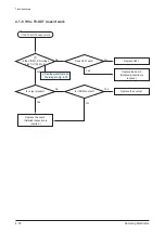
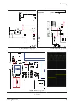
Page 21: ...ent Yes No Does U701 work Does U301 work Replace U701 No No Yes Replace the board Detailed inspection is required 4 1 2 If there is no sound Yes Yes If there is no sound Replace U301 No Replace the board Detailed inspection is required See the waveform and the image in Fig 4 4 ...

Page 22: ...ND U702 FDMA1028NZ 1 S1 2 G1 3 D2_1 4 S2 5 G2 6 D1_1 7 D1_2 8 D2_2 R715 560 R714 560 LOUT_EP MUTE GND ROUT_EP C721 330uF 2 5V C722 330uF 2 5V C718 100nF GND R711 200K AUDIO CODEC page 7 6 U701 U504 U801 U101 U702 U507 U506 U401 MAIN PCB Top page 6 1 Fig 4 4 ...

Page 23: ...ncel the HOLD status by pressing the power key on the main body Disassemble the main body and check if the TOUCH FPCB is connected correctly or faulty If the touch pad is faulty replace it Replace the board Detailed inspection is required Yes No Yes No Yes No If the touch pad doesn t work 4 1 3 If the touch pad doesn t work ...

Page 24: ...o signal present Yes No Does U701 work Does X402 work Replace U701 No No Yes Replace the board Detailed inspection is required 4 1 4 If FM doesn t work Yes Yes If FM doesn t work Replace X402 No Replace the board Detailed inspection is required See the waveform and the image in Fig 4 5 ...

Page 25: ...RT_RXD C8 UART_TXD D7 UART_RTS_N E8 UART_CTS_N F7 SCL E7 SDA A8 SPIM_CLK C7 SPIM_CS_N F6 PCM_IN G6 PCM_OUT F4 PCM_CLK F5 PCM_SYNC B6 COEX_IN E4 COEX_OUT0 E5 COEX_OUT1 B1 VDDIF C1 VDDTF E1 VDDLNA F1 VDDRF G1 VDDPX A5 VDDC_1 B8 VDDC_2 F8 VDDC_3 G5 VDDO_1 A6 VDDO_2 G8 VDDO_3 C2 VSS_1 D2 VSS_2 F2 VSS_3 D3 VSS_4 C6 VSS_5 A7 VSS_6 G7 VSS_7 C121 2200nF C122 2200nF R111 100K R118 1K C120 4700nF R115 100K ...

Page 26: ...IMMING ports voltages high Are the FPCB and the connector connected properly Connect the LCD FPCB and the connector properly Disassemble the main body and replace the LCD Replace the board Detailed inspection is required Yes No Yes No If the LCD displays nothing See the waveform and the image in Fig 4 6 ...

Page 27: ...200K P_3 0V C631 470nF 10V R641 200K CORE_CTL C612 10000nF 10V Q602 KTK5132V 1 Source 2 Gate 3 Drain GND P_3 0V C618 1000nF VD602 14V R618 4 7K R624 56K R625 270K 1 GND C630 100nF P_1 8V U604 MAX17040G T 1 CTG 2 CELL 3 VDD 4 GND 5 SEO 6 EO 7 SCL 8 SDA C625 1000nF L604 10uH R604 10K R622 10K R631 100K R612 100K R640 100K R621 100K R628 100K C615 22000nF ON CON ON R609 10K R613 10K P_1 8V C634 1000n...

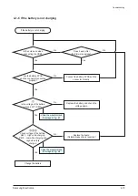
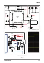
Page 28: ...ove 4 5V C801 Yes Replace the battery and check the voltage again No Replace the board Detailed inspection is required Is the screen on when connecting the USB If the battery is not charging 2 3 4 Check voltage of the battery R621 High while charging R618 Low while charging and High when fully charged Yes No Connect the battery FPCB and the connector properly No See the waveform and the image in F...

Page 29: ...N_BATT C803 100nF R815 10K GND C801 2200nF 10V D801 ESD7L5 0DT5G 9 10 11 12 13 14 15 16 17 18 19 20 21 22 23 24 C802 1000nF U801 NCP360SNT1G 1 IN 2 GND 3 EN 4 FLAG 5 OUT D802 uClamp1201P TCT R808 3 9ohm R810 3 9ohm 24PIN IO INTERFACE page 7 7 U701 U504 U801 U402 U101 U702 U507 U506 U604 U401 MAIN PCB Top page 6 1 Fig 4 7 ...

Page 30: ... R603 270K R633 150 R632 150 R616 39K R639 200K P_3 0V C631 470nF 10V R641 200K CORE_CTL C612 10000nF 10V Q602 KTK5132V 1 Source 2 Gate 3 Drain GND P_3 0V C624 22000nF 6 3V VD602 14V R618 4 7K R624 56K R625 270K 1 GND U604 MAX17040G T 1 CTG 2 CELL 3 VDD 4 GND 5 SEO 6 EO 7 SCL 8 SDA L604 10uH R630 10K R622 10K R631 100K R612 100K R640 100K R621 100K R628 100K C615 22000nF L603 4 7uH L601 4 7uH L602...

Page 31: ...Is the bias voltage present R704 1 5V Does the MIC look fine when checking visually Replace the MIC Disassemble the main body and replace the MIC Replace the board Detailed inspection is required Yes No Yes No If the MIC doesn t work properly See the waveform and the image in Fig 4 9 ...

Page 32: ... WM1808 1 LIP 2 LIN 3 L2 GPIO2 4 R2 GPIO3 5 DACDAT 6 LRC 7 BCLK 8 ADCDAT 9 MRCK 10 DGND 11 DCVDD 12 DBVDD 13 CSB GPIO1 14 SCLK 15 SDIN 16 MODE 17 AUXL 18 AUXR 19 OUT3 20 ROUT2 21 AGND2 22 LOUT2 23 AVDD2 24 VMID 25 AGND1 26 ROUT1 27 LOUT1 28 AVDD1 F GND C702 100nF I2 LOUT_EP P_3 0V C705 1000nF C701 1000nF C714 1000nF C707 22000nF R710 47K R705 10K L704 600ohm R709 10K R708 10K C704 2200nF C716 4700...

Page 33: ... 6 Yes No Does U301 work Is it DRM content Replace U301 No No Yes Replace the board Detailed inspection is required 4 1 8 If the TV OUT doesn t work Yes No If the TV OUT doesn t work Replace the content Yes Replace the board Detailed inspection is required See the waveform and the image in Fig 4 10 ...

Page 34: ...T_L C713 100nF 08 12 DBVDD 13 CSB GPIO1 14 SCLK 15 SDIN 16 MODE 17 AUXL 18 AUXR 19 OUT3 20 ROUT2 21 AGND2 22 LOUT2 23 AVDD2 24 VMID FM_LINE_IN_L LINE_OUT_R I2C_DAT0 LOUT_EP C714 1000nF C718 100nF C715 1000nF R709 10K R708 10K R717 100K VIDEO_DACOUT R707 75 GND VIDEO_EN VIDEO_OUT P_3 0V C723 100nF R711 200K U704 FSM6151L6X_F113 1 VIN 2 GND 3 SAG 4 VOUT 5 VCC 6 EN AUDIO CODEC page 7 6 CON901 CON601 ...

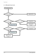
Page 35: ...ace X101 No No Yes Replace the board Detailed inspection is required 4 1 9 If Bluetooth doesn t work Yes Yes If Bluetooth doesn t work Replace U102 No Replace the board Detailed inspection is required Is the Bluetooth antenna fine Yes Replace ANT101 No See the waveform and the image in Fig 4 11 See the waveform and the image in Fig 4 11 ...

Page 36: ...OUT P_3 0V GND C107 100nF GND P_1 8V REG_BT GND R105 1K BT_WAKE BT_RST AUD_DATA_IN REG_BT REG_BT GND GND BT_UART_RX0 BT_UART_TX0 AUD_LRCK AUD_BCLK L101 8 2nH B101 600ohm BT_UART_RTS0 BT_UART_CTS0 R102 100K C123 100nF R107 15K R101 47K R108 47K C105 1000nF C106 1000nF SI4709 B GMR 5 SE 6 SC 7 SD 8 VI AUD_DATA_OUT U102 BCM2070CB0KUFBXG G4 RES D1 RFP G2 XIN G3 XOUT A4 LPO_IN B2 REG_EN A3 VBAT A2 VREG...

Page 37: ...ion displayed on the LCD Complete Install a driver and check it again Yes No Yes Yes Is Unknown device present in the device manger Delete and update it with Upgrade Tool and check if it works No No Yes No Can you format on the browser No Replace the Board Yes Yes Yes No No Can you access Connect USB Reset and check if USB connection is displayed ...

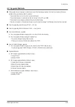
Page 38: ...touch_fw bin How to main firmware upgrade A You can upgrade firmware copying R1 rom on the YP R1 s file directory B You can upgrade firmware using R1 Update Tool You will use B way if A way make trouble This way can low level format and optimize the YP R1 How to TOUCH firmware upgrade C You can upgrade firmware copying touch_fw bin on the YP R1 s file directory You should upgrade TOUCH firmware if...

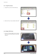
Page 39: ...Copy R1 rom A 1 1 Copy the R1 rom on the YP R1 s file directory 2 Paste the R1 rom to the root director of the YP R1 4 2 2 Reboot YP R1 A 2 1 You can see Firmware Update on the screen and then menu will come into being on the screen after upgrading ...

Page 40: ...ectronics 4 25 Troubleshooting 4 2 3 Install Driver B 1 1 Double click on the file below to execute the driver installation windriver wd_install_4NT bat If driver is already installed you do not need to reinstall ...

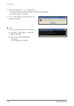
Page 41: ...oing R1 Update Tool exe program If you did this already do not install If vc_s1_redist_x86 exe makes error like this use another way to install Install 1 vc_s1_redist_x86 exe file to C root directory 2 Click Start Click Run R Input cmd Enter or Click OK 3 Input next command at DOS window cd c Enter vc_s1_redist_x86 exe t c Enter ...

Page 42: ... Troubleshooting 4 2 4 Enter Firmware Upgrade Mode B 2 1 SET should be bootstrap mode for upgrading firmware 2 How to be 1 Connect PC and SET by USB Cable 2 When you pushing the power button press the reset button at 5 seconds ...

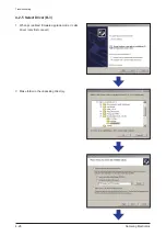
Page 43: ...4 28 Samsung Electronics Troubleshooting 4 2 5 Select Driver B 3 1 When pc realized firmware upgrade mode it calls driver only first connect Make folder in the unpacking directory ...

Page 44: ...Samsung Electronics 4 29 Troubleshooting Install completed Check device manager ...

Page 45: ...Update Tool exe file in the Upgrade Tool folder Check if you want to erase NAND all 2 Choose the firmware R1 ROM is in the firmware realease 3 You can upgrade all if you choose each images that Mboot Linux Root File System file Skip image Mboot or Linux or Root File System if you don t need to upgrade ...

Page 46: ... see the message that completed after 5 minutes almost 6 If you want to erase NAND push the Erase Nand button and then upgrade Check if you want to erase all data in NAND flash memory Situation to erase NAND SET doesn t work can t booting Install Method of release note needs to Erase Check if you want to erase all data in NAND flash memory ...

Page 47: ...4 2 7 Copy touch_fw bin C 1 1 Copy touch_fw bin on the YP R1 s file directory 2 Paste the touch_fw bin file to the root directory of the YP R1 4 2 8 Reboot YP R1 C 2 1 You can see Touch Sensor Updating on the screen and then screen will be off ...

Page 48: ...MEMO Samsung Electronics 4 33 ...

Page 49: ...Electronics Exploded View Part List This Document can not be used without Samsung s authorization 5 Exploded View Part List 5 1 Exploded View QMP01 QME04 QVO03 QFM01 QVO01 QBD01 QBR01 QJA01 QSM09 QLC01 QBA01 QCP01 ...

Page 50: ...R ASS Y 1 SA QCP01 AH63 01972A CUSHION PCB YP R1 PORON 1 2mm 30 23 BLAC 1 SA QFM01 GM61 01016A HOLDER FRAME YP R1 PC 43 81 BLACK 1 SA QJA01 GM63 01030A COVER JACK YP R1 PC 43 8 9 BLACK 1 SA QLC01 GM96 01009A ELA ETC YP R1 LCD ASS Y YP R1 SAMSUNG LC 1 SA QME04 AH97 03272B ASSY FRAME TOUCH MP3 YP R1 WINDOW TSP KN 1 SA QMP01 GM92 01022A ASSY PBA MAIN YP R1 WORLDWIDE 4GB 1 SA QSM09 6003 001660 SCREW T...

Page 51: ...W TP 1005 1 SNA 2007 007697 R CHIP 2 4Kohm 1 1 16W TP 1005 1 SNA 2007 007942 R CHIP 1Mohm 1 1 16W TP 1005 1 SA 2007 008167 R CHIP 120Kohm 1 1 16W TP 1005 1 SA 2007 008294 R CHIP 33ohm 1 1 16W TP 1005 1 SNA 2007 010185 R CHIP 3 9ohm 1 1 16W TP 1005 3 SNA 2011 001262 R NETWORK 22ohm 5 1 16W L CHIP 8P 1 SA 2011 001396 R NETWORK 4 7Kohm 5 1 16W L CHIP 8 3 SNA 2203 000254 C CER CHIP 10nF 10 16V X7R TP ...

Page 52: ...80 L140 TRP 4 PE 1 SA QCP01 AH63 01972A CUSHION PCB YP R1 PORON 1 2mm 30 23 1 SA AH68 00511G LABEL SEAL YP Z5F ART PAPER 1 SA GM63 01086ASHEET WINDOW YP R1 P E T 0 05 35 50 1 SNA GM74 01005ATAPE CONNECTOR YP R1 110PE 9 7 17 5 2 SNA QBA01 4302 001229 BATTERY POLYMER 3 7V 500mAH CELL 20 1 SA AH68 00508U LABEL SERIAL COMMON ELS 90 1 SA Loc No Part No Description Specification Q ty SNA Remark Loc No P...

Page 53: ...5 5 Samsung Electronics MEMO ...

Page 54: ...1 24MHz Crystal Main CLK 2 Finger GASKET Improved resistance to ESD 3 32 768KHz Crystal Bluetooth CLK 4 FM Tuner IC Supports reception of FM signals 5 CODEC IC Supports voice codec TP1 1 4 5 2 3 TP4 TP5 TP2 TP3 TP8 TP5 TP7 TP6 TP6 TP6 U701 U504 U801 U402 U101 U702 U507 U506 U604 U401 ...

Page 55: ...6 2 Samsung Electronics PCB Diagram 6 1 1 Test Point Wave Form TP1 TP2 TP3 TP4 TP5 TP6 TP8 TP7 ...

Page 56: ...CB and the touch pad using the FPCB 7 Earphone Jack 8 USB Connector Cable port for communication with external devices 9 MIC Supports voice recording 0 Main IC ARM1176 Core 600MHz RTC module are built in Controls overall system functions Mobile DDR SDRAM IC Supports data transfer in the system PM IC Battery charger and dual buck converter are built in Battery connector Connects and holds the batte...

Page 57: ...TERY DETECT 24 PBA_CE 7 J701 Earphone Jack Pin No Signal 1 GROUND 2 R CH 3 L CH 6 CON802 Touch PAD Connector Pin No Signal 1 GROUND 2 GROUND 3 GROUND 4 T_RESET 5 T_DATA 6 T_CLK 7 VCC 8 VCC 2 CON901 LCD Connector Pin No Signal Pin No Signal 1 GND 21 LCD_D 15 2 LCD_CE 22 LCD_RST 3 LCD_RS 23 GND 4 LCD_WR 24 VDD_IO 5 LCD_RD 25 VDD_IO 6 LCD_D 0 26 GND 7 LCD_D 1 27 VDD_IO 8 LCD_D 2 28 VDD_IO 9 LCD_D 3 2...

Page 58: ...Samsung Electronics 6 5 PCB Diagram 6 2 2 Test Point Wave Form TP2 TP3 TP4 TP7 TP6 ...

Page 59: ...6 6 Samsung Electronics MEMO ...

Page 60: ...rial BAT PMIC MAX1819 BT_3 0V P_1 8V ANT 50 ohm TOUCH PAD DC DC 3 CH BUCK P_3 0V P_1 8V P_3 0V P_1 2V LED Driver STEP UP CHARGER RESET OSC RTC RTC BAT Processor i MX37 32bit ARM1176 600Mhz AUDIO TV OOUT 3 5φ JACK Main System has basic circuit blocks e g Processor i MX37 Mobile DDR RAM Flash Memory Power Block Audio DAC and a block for the FM Tuner The display is connected to a 2 6 inch QVGA TFT LC...

Page 61: ...M_A0 D6 ETM_D7 EIM_DA15 DRAM_D31 E7 ETM_D6 EIM_DA14 DRAM_D30 E6 ETM_D5 EIM_DA13 DRAM_D29 D5 ETM_D4 EIM_DA12 DRAM_D28 E5 ETM_D3 EIM_DA11 DRAM_D27 D4 ETM_D2 EIM_DA10 DRAM_D26 B3 ETM_D1 EIM_DA9 DRAM_D25 F5 ETM_D0 EIM_DA8 DRAM_D24 B2 KEY_ROW7 EIM_DA7 DRAM_D23 B1 KEY_ROW6 EIM_DA6 DRAM_D22 C2 KEY_ROW5 EIM_DA5 DRAM_D21 C1 KEY_ROW4 EIM_DA4 DRAM_D20 D2 KEY_ROW3 EIM_DA3 DRAM_D19 D1 KEY_ROW2 EIM_DA2 DRAM_D18...

Page 62: ...G_RST_B_DEB R9 UART2_RXD_MUX GPIO2_31 V8 UART2_TXD_MUX GPIO2_30 P9 UART2_RTS_MUX GPIO2_29 W8 UART2_CTS W9 GPIO2_27 V9 GPIO2_26 T9 UART_TX1 GPIO2_25 V10 UART_RX1 GPIO_24 T6 CSPI2_SCLK I2C3_SCLK GPIO3_9 W4 CSPI2_SS1 GPIO3_8 V5 CSPI2_SS0 GPIO3_7 W5 CSPI2_MISO GPIO3_6 R7 CSPI2_MOSI I2C3_SDA GPIO3_5 T7 CSPI1_SCLK I2C1_SCL GPIO3_4 V6 CSPI1_SS1 GPIO3_3 R8 CSPI1_SS0 GPIO3_2 W6 CSPI1_MISO GPIO3_1 V7 CSPI1_...

Page 63: ... B6 NAND_R B1 NAND_R B0 NAND_R B2 NAND_R B3 NAND_R B0 NAND_R B1 NAND_R B2 NAND_R B3 NAND_R B4 NAND_R B5 NAND_R B7 NAND_R B6 P_3 0V R505 4 7K R506 4 7K C511 100nF C507 100nF C510 100nF C503 100nF C522 100nF C525 100nF C523 100nF C524 100nF GND C520 100nF R504 4 7K R502 4 7K R507 10K P_3 0V GND NAND_SELECT U501 K4X51323PG 8GC6 H3 A12 H2 A11 J7 A10 H1 A9 J3 A8 J2 A7 J1 A6 K3 A5 K1 A4 K9 A3 K7 A2 J9 A...

Page 64: ... P_3 0V C624 22000nF 6 3V C618 1000nF VD602 14V R618 4 7K GND VDDA_1 2V R624 56K R625 270K 1 GND LP_CTL C630 100nF P_1 8V U604 MAX17040G T 1 CTG 2 CELL 3 VDD 4 GND 5 SEO 6 EO 7 SCL 8 SDA C625 1000nF L604 10uH R630 10K R604 10K R622 10K R631 100K R612 100K R640 100K R621 100K R628 100K C615 22000nF V_DDCON V_DDCON V_DDCON GND GND R609 10K R613 10K P_1 8V C634 1000nF R607 100K C603 2200nF P_2 5V P_3...

Page 65: ...CLK P_3 0V LINE_OUT_L GND AUD_DATA_IN C713 100nF U701 WM1808 1 LIP 2 LIN 3 L2 GPIO2 4 R2 GPIO3 5 DACDAT 6 LRC 7 BCLK 8 ADCDAT 9 MRCK 10 DGND 11 DCVDD 12 DBVDD 13 CSB GPIO1 14 SCLK 15 SDIN 16 MODE 17 AUXL 18 AUXR 19 OUT3 20 ROUT2 21 AGND2 22 LOUT2 23 AVDD2 24 VMID 25 AGND1 26 ROUT1 27 LOUT1 28 AVDD1 FM_LINE_IN_L GND LINE_OUT_R C702 100nF I2C_DAT0 LOUT_EP P_3 0V C705 1000nF C701 1000nF C714 1000nF C...

Page 66: ... R820 47K GND C801 2200nF 10V D801 ESD7L5 0DT5G CON801 24P 1 2 3 4 5 6 7 8 9 10 11 12 13 14 15 16 17 18 19 20 21 22 23 24 CON802 8P 1 2 3 4 5 6 7 8 R817 4 7K R809 0 R801 0 P_3 3V C802 1000nF R806 150 R804 150 C804 100nF R802 22 TOUCH_CE R807 100K R811 3 9ohm U801 NCP360SNT1G 1 IN 2 GND 3 EN 4 FLAG 5 OUT D802 uClamp1201P TCT R808 3 9ohm R810 3 9ohm POWER HOLD 14 Uart TX1 22 BATT 4 ADAPTOR 15 USB D ...

Page 67: ...LCD_DATA_IN LCD_DATA_OUT R905 22 CON901 43P 1 2 3 4 5 6 7 8 9 10 11 12 13 14 15 16 17 18 19 20 21 22 23 24 25 26 27 28 29 30 31 32 33 34 35 36 37 38 39 40 41 42 43 INN_BATT UART_TX1 FM_ANT EP_TEST_L EP_TEST_R UART_RX1 CON902 1 2 3 4 5 6 7 8 9 10 11 12 13 14 15 16 USB_D USB_D USB_P5V PWR_IN_DDCON GND PBA_CE LCD_GRN7 GND C902 1000nF R901 33 R903 100K GND GND GND SCR 1 R909 1K F2 ICT 04 001 1 2 3 F3 ...

Page 68: ... VBAT A2 VREGHV A1 VREG B4 RST_N C4 TM0 F3 TM2 B5 GPIO_0 B3 GPIO_1 E6 GPIO_5 E3 GPIO_6 B7 GPIO_7 D8 UART_RXD C8 UART_TXD D7 UART_RTS_N E8 UART_CTS_N F7 SCL E7 SDA A8 SPIM_CLK C7 SPIM_CS_N F6 PCM_IN G6 PCM_OUT F4 PCM_CLK F5 PCM_SYNC B6 COEX_IN E4 COEX_OUT0 E5 COEX_OUT1 B1 VDDIF C1 VDDTF E1 VDDLNA F1 VDDRF G1 VDDPX A5 VDDC_1 B8 VDDC_2 F8 VDDC_3 G5 VDDO_1 A6 VDDO_2 G8 VDDO_3 C2 VSS_1 D2 VSS_2 F2 VSS_...

Page 69: ...7 10 Samsung Electronics MEMO ...

Reviews: