COMe-cVR6 – User Guide Rev. 1.5
// 58
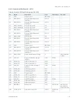
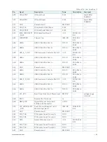
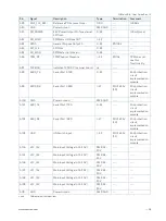
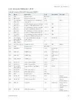
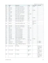
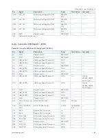
Pin
Signal
Description
Type
Termination
Comment
A89
PCIE_CLK_REF-
Reference PCI Express Clock -
DP-O
---
100MHz
A90
GND
Power Ground
PWR GND
---
---
A91
SPI_POWER
3.3V Power Output Pin for external
SPI flash
O-3.3
---
100mA (max.)
A92
SPI_MISO
SPI Master IN Slave OUT
I-3.3
---
A93
GPO0
General Purpose Output 0
O-3.3
PD 100k
---
A94
SPI_CLK
SPI Clock
O-3.3
---
---
A95
SPI_MOSI
SPI Master Out Slave In
O-3.3
---
---
A96
TPM_PP
TPM Physical Presence
I-3.3
PD 10k
TPM does not
use this
functionality
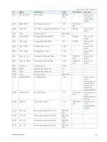
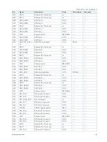
A97
TYPE10#
Indicates TYPE10# to carrier board
nc
---
---
A98
SER0_TX
Serial Port 0 TXD
O-3.3
---
20V protection
circuit
implemented on
module
A99
SER0_RX
Serial Port 0 RXD
I-5T
PU 47k 3.3V
(S0)
20V protection
circuit
implemented on
module
A100
GND
Power Ground
PWR GND
---
---
A101
SER1_TX
Serial Port 1 TXD
O-3.3
---
20V protection
circuit
implemented on
module
A102
SER1_RX
Serial Port 1 RXD
I-5T
PU 47k 3.3V
(S0)
20V protection
circuit
implemented on
module
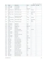
A103
LID#
LID Switch Input
I-3.3
PU 47k 3.3V
(S5)
20V protection
circuit
implemented on
module
A104
VCC_12V
Main Input Voltage (4.75-20V)
PWR 8.5-
20V
---
---
A105
VCC_12V
Main Input Voltage (4.75-20V)
PWR 8.5-
20V
---
---
A106
VCC_12V
Main Input Voltage (4.75-20V)
PWR 8.5-
20V
---
---
A107
VCC_12V
Main Input Voltage (4.75-20V)
PWR 8.5-
20V
---
---
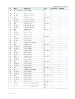
A108
VCC_12V
Main Input Voltage (4.75-20V)
PWR 8.5-
20V
---
---
A109
VCC_12V
Main Input Voltage (4.75-20V)
PWR 8.5-
20V
---
---
A110
GND
Power Ground
PWR GND
---
---
+ and -
Differential pair differentiator


