2-1-2. Terminal Voltages of CCD lmager
The terminal voltages of the CCD imager are given in Table
2-1 .
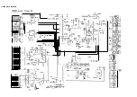
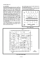
In order to input a signal that has the specified timing and
voltage for these terminals, a timing IC (IC91 6, CXD1 256R)
for generation of vertical and horizontal transfer clocks and
a PG clock and V driver IC (IC91 8, CXD1250N) are
necessary. The block diagram is shown in Fig. 2-3.
Pin No.
Symbol
Pin Description
1
V4
Vertical register transfer clock
2
V3
Vertical register transfer clock
3
V2
Vertical register transfer clock
4
V1
Vertical register transfer clock
5
GND
GND
7
Vss
Output amplifier source
6
VGG
Output amplifier gate bias
8
OUT
Signal output
9
Voo
Output amplifier drain bias
1 0
GND
GND
1 1
SUB
Overflow drain voltage
1 2
VL
Protection transistor bias
1 3
PG
Pre-charge gate clock
1 4
LH 1
Horizontal register final transfer clock
1 5
H1
Horizontal register transfer clock
1 6
H2
Horizontal register transfer clock
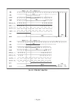
XV1 to XV4 are the vertical transfer clock. In order to obtain
a 3-value pulse, XSG1 and XSG2 are overlapped on XV1
and XV3. XSUB is the throwaway pulse for electronic
shutter operations. H1 and H2 are the horizontal transfer
clock, and PG is the pre-charged gate clock.
The pin functions are shown in Table 2-2.
Waveform
Voltage
_Il___Il___fi__
-8.5 V, O V
-8.5 V, 0 V, 1 5 V
LJ1J1.JlJ
- 8.5 V, O V
-8.5 V, 0 V, 1 5 V
GND
O V
DC (self bias)
4 V
DC
Approx. 1 0 V
DC
1 5
v
GND
o v
DC
Adjustment value
(Adjustment value,
(
....n________n_ )
*
value +24
DC
-8.5 V
__/\__A_
Adjustment value,
adjustment value +5 V
__J\__J\_
O V, 5 V
__J\__J\_
O V, 5 V
O V, 5 V
Table. 2-1 . CCD Terminal Voltage
( )
*
In the electronic shutter mode
IC951 (CCD)
IC918(V DRIVER)
IC91 6(TIMING)
IC932
IC931
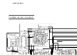
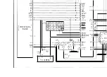
Fig. 2-3. CCD Drive Circuit Block Chart
- 4-1 0 -
SCK}
System control
so


