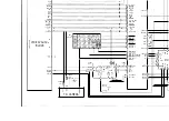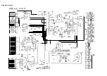
2-3. IC91 7 (Fig. 2-1 7.)
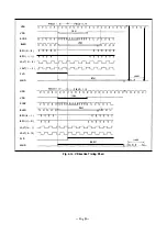
2-3-1 . CDS Circuit
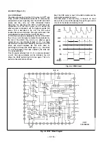
The video signal output from the CCD is input to Pin ® and
Pin @ of IC91 7 (CXA 1 390AR). Inside this IC, there are five
sample/hold circuits originating form the XSHP and XSHD
pulses, and they carry out CDS (Correlated Double
Sampling). The objective of the CDS is to eliminate noise
components from the CCD output, and to extract the
effective signal components with the highest possible S/N
status. This is described in Fig. 2-5. The CCD output
includes black level information and signal component, and
noise effected by a leak from the harmful PG clock.
In CDS, the black level is detected by the S/H of the XSHP
(Fig. 2-5 ® ), and the signal components are detected by
the S/H of the XSH D (Fig. 2-5
®
). An effective signal
component can be obtained through
®
-
® ,
but these
signals would include noise effected by the drain of the S/H
pulse, and would decrease the S/N ratio. Here, by
performing S/H through the XSHD again in ® , it becomes
® ,
and the phases of the noise created by the drain and
®
can be combined.
From the signal obtained from
®- ® ,
a signal component
® with the noise eliminated can be obtained. Fig. 2-6
shows the XSHP performing S/H once again. This is to
perform a finer elimination of noise.
CCD
Next, the CDS output is input to the AGC amplifier and the
high luminance detection circuit.
The CDS output is fed from Pin @ to the auto iris circuit
and auto focus circuit after passing through the gain control
circuit and the clamp and blanking circuits.
CCD
output
XSHP
XSHD
®
@
©
@
!©-®l
IRIS. AF
Fig. 2-5. CDS Circuit
cs
F3
F2
F1
GY
IC91 7
CXA1 390AR
Fig. 2-6. IC91 7 Block Diagram
- 4-1 3 -


