


- 56 -
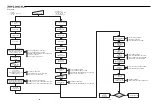
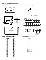
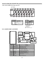
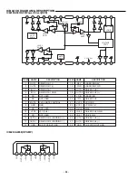
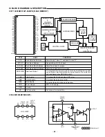
IC BLOCK DIAGRAM & DESCRIPTION
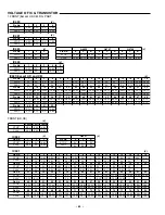
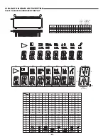
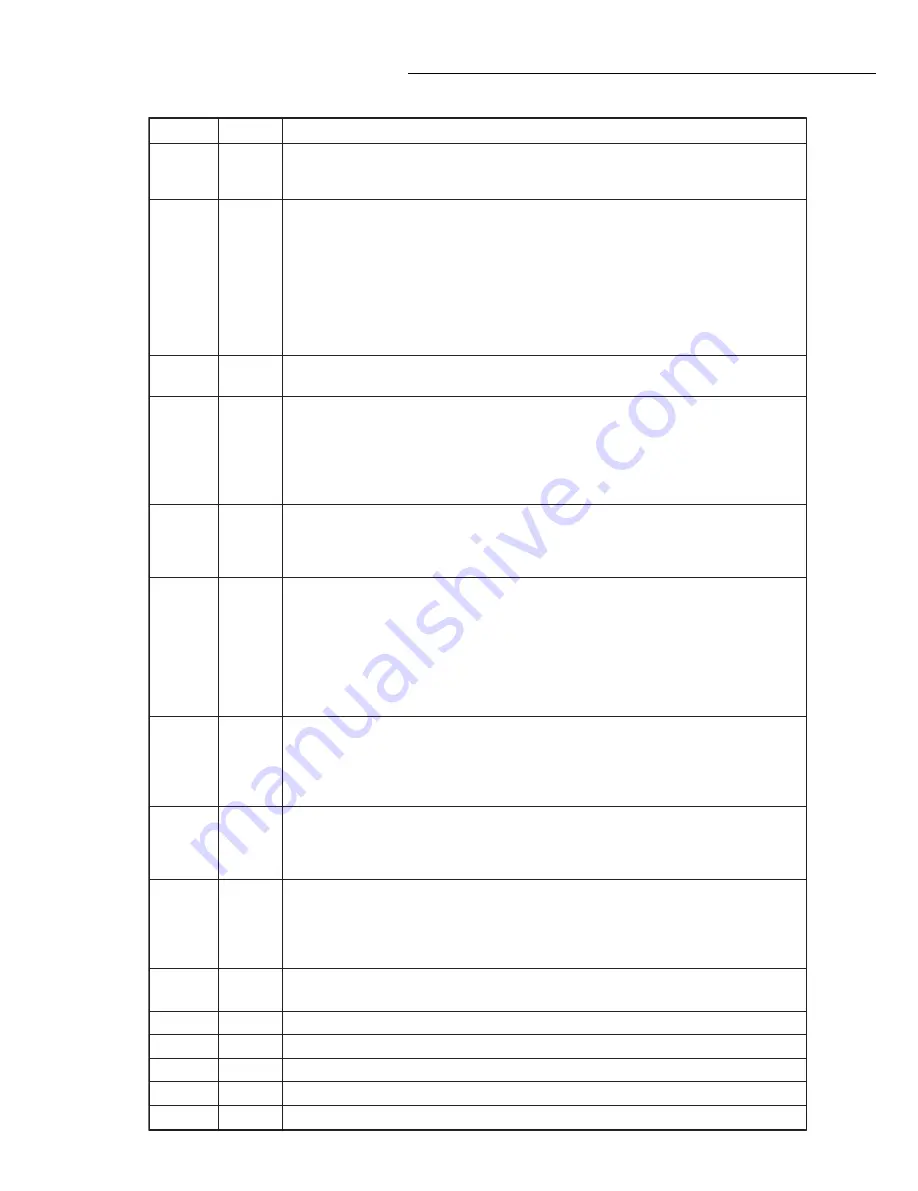
IC806,807 EM636165TS-8(SDRAM)
Symbol
Type
Description
CLK
Input
Clock: CLK is driven by the system clock. All SDRAM input signals are sampled on
the positive edge of CLK. CLK also increments the internal burst counter and controls
the output registers.
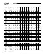
CKE
Input
Clock Enable: CKE activates(HIGH) and deactivates(LOW) the CLK signal.If CKE
goes low synchronously with clock(set-up and hold time same sa other inputs), the
internal clock is suspended from the next clock cycle and the state of output and
burst address is frozen as long as the CKE remains low. When both banks are in the
idle state, deactivating the clock controls the entry to the Power Down and Self Refresh
modes. CKE is synchronous except after the device enters Power Down and Self
Refresh modes, where CKE becomes asynchronous until exiting the same mode.
The input buffers, including CLK, are disabled during Power Down and Self Refresh
modes, providing low standby power.
A11
Input
Bank Select: A11(BS) defines to which bank the BankActivate, Read, Write, or
BankPrecharge command is being applied.
AC-A10
Input
Address Inputs: A0-A10 are sampled during the BankActivate command (row address
A0-A10 and Read/Write command (column address A0-A7 with A10 defining Auto
Precharge) to select one location out of the 256K available in the respective bank.
During a Precharge command, A10 is sampled to determine if both banks are to be
precharged (A10-HIGT). The address inputs also provide the op-code during a Mode
Register Set command.
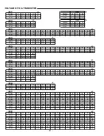
CS#
Input
Chip Select: CS# enables (sampled LOW) and disables (sampled HIGH) the command
decoder. All commands are masked when CS# is sampled HIGH. CS# provides for
external bank selection on systems with multiple banks. It is considered part of
the command code.
RAS#
Input
Row Address Strobe: The RAS# signal defines the operation commands in conjunction
with the CAS# and WE# signals and is latched at the positive edges of CLK. When
RAS# and CS# are asserted "LOW" and CAS# is asserted "HIGH," either the
BankActivate command or the Precharge command is selected by the WE# signal.
When the WE# is asserted "HIGH," the BankActivate command is selected and the
bank designated by BS is turned on to the active state. When the WE# is asserted
"LOW," the Precharge command is selected and the bank designated by BS is
switched to the idle state after the precharge operation.
CAS#
Input
Column Address Strobe: The CAS# signal defines the operation commands in
conjunction with the RAS# and WE# signals and is latched at the positive edges of
CLK. When RAS# is held "HIGH" and CS# is asserted "LOW," the column access is
started by asserting CAS#"LOW." Then, the Read or Write command is selected by
asserting WE# "LOW" or "HIGH."
WE#
Input
Write Enable: The WE# signal defines the operation commands in conjunction with
the RAS# and CAS# signals and is latched at the positive edges of CLK. The WE#
input is used to select the BankActivate or Precharge command and Read or Write
command.
LDQM,
UDQM
Input
Data Input/Output Mask: LDQM and HDQM are byte specific, nonpersistent I/O buffer
controls. The I/O buffers are placed in a high-z state when DQM is sampled HIGH.
Input data is masked when DQM is sampled HIGH during a write cycle. Output data
is masked (two-clock latency) when DQM is sampled HIGH during a read cycle.
UDQM masks DQ15-DQ8, and LDQM masks DQ7-DQ0.
DQC-DQ15 Input /
Output
Data I/O: The DQ0-15 input and output data are synchronized with the positive edges
of CLK. The I/Os are byte-maskable during Reads and Writes.
NC
-
No Connect: These pins should be left unconnected.
V
DDQ
Supply
DQ Power: Provide isolated power to DQs for improved noise immunity.(3.3V+/-0.3V)
V
SSQ
Supply
DQ Ground: Provide isolsted ground to DQs for improved noise immunity.(0V)
V
DD
Supply
Power Supply: +3.3V+/-0.3V
V
SS
Supply
Ground
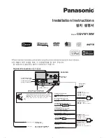
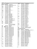
Summary of Contents for 137 103 01
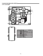
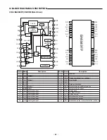
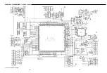
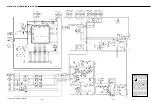
Page 47: ...SCHEMATIC DIAGRAM MPEG for AU SS and CA This is a basic schematic diagram 64 65 ...
Page 48: ...SCHEMATIC DIAGRAM MPEG for XE UK This is a basic schematic diagram 66 67 ...
Page 53: ...SANYO Technosound Co Ltd Osaka Japan Apr 01 3500 BB Printed in Japan ...
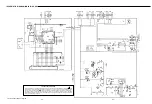
Page 61: ...MPEG P W BOARD SCHEMATIC DIAGRAM FOR WAVEFORM CHECK This is a basic waveform check 32 33 ...
Page 62: ...AMP P W BOARD SCHEMATIC DIAGRAM FOR WAVEFORM CHECK This is a basic waveform check 34 35 ...
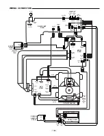
Page 63: ...WIRING DIAGRAM MPEG A SIDE 68 69 ...
Page 64: ...WIRING DIAGRAM MPEG B SIDE 70 71 ...
Page 65: ...WIRING DIAGRAM DG SOCKET POWER SW for AU SS 74 75 DG SOCKET POWER SW ...
Page 66: ...WIRING DIAGRAM FRONT for AU SS 76 77 ...
Page 67: ...WIRING DIAGRAM DG SOCKET POWER SW for XE UK 80 81 DG SOCKET POWER SW SCART SW ...
Page 68: ...WIRING DIAGRAM FRONT for XE UK 82 83 ...
Page 69: ...WIRING DIAGRAM DG SOCKET POWER SW for CA 86 87 DG SOCKET POWER SW ...
Page 70: ...WIRING DIAGRAM FRONT for CA 88 89 ...
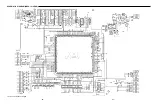
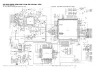
Page 72: ...SCHEMATIC DIAGRAM DVD TOP LEFT This is a basic schematic diagram 92 93 ...
Page 73: ...SCHEMATIC DIAGRAM DVD BOTTOM LEFT This is a basic schematic diagram 94 95 ...
Page 74: ...SCHEMATIC DIAGRAM DVD TOP RIGHT This is a basic schematic diagram 96 97 ...
Page 75: ...SCHEMATIC DIAGRAM DVD BOTTOM RIGHT This is a basic schematic diagram 98 99 ...