- 30 -
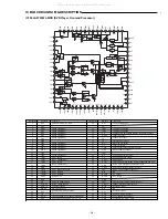
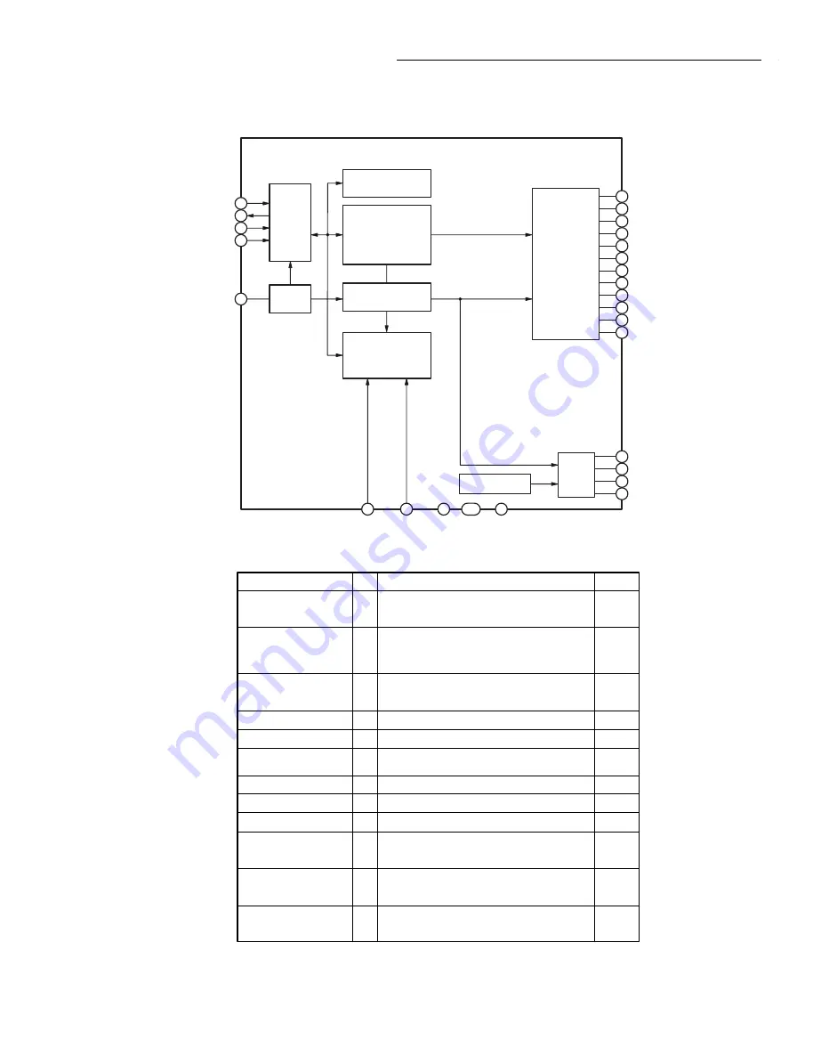
IC BLOCK DIAGRAM & DESCRIPTION
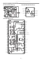
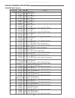
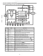
IC831 PT6313-S(LED Driver)
OSC
Serial
Data
Interface
7
8
9
10
11
12
13
14
16
17
18
19
23
22
21
20
28
27
1
2
26
15
5,25
6
4
3
Control
Display Memory
Key Matrix Memory
Grid
Driver
Segment
Driver/
Grid
Driver/
Key Scan
Output
Dimming Circuit
Timing Generator
SG1/KS1
SG2/KS2
SG3/KS3
SG4/KS4
SG5/KS5
SG6/KS6
SG7/KS7
SG8/KS8
SG9/GR8
SG10/GR7
SG11/GR6
SG12/GR5
GR1
GR2
GR3
GR4
DIN
DOUT
CLK
STB
OSC
VEE
GND
VDD
K2
K1
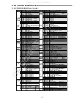
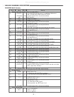
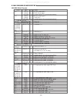
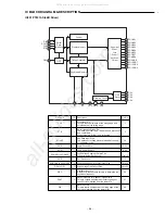
Description
Clock Input Pin
This pin reads serial data at the rising edge and
outputs data at the falling edge
Serial Interface Strobe Pin
The data input sfter the STB has fallen is processed
as a command
When this pin is "HIGH" CLK is ignored
Key Data Input Pins
The data sent to these pins are latched at the end
of the display cycle
Logic Ground Pin
Logic Power Supply
High Voltage Segment Output Pins
Also acts as the Key Souree
Pull Down Level
High voltage Segment/Grid Output Pins
High Voltage Grid Output Pins
Oscillator Input Pin
A resistor is connected to this pin to determine the
oscillation frequency
Data Output Pin (N-Channel, Open Drain)
This pin outputs serial data at the falling edge of
the shift clock (starting from the lower bit)
Data Input Pin
This pin inputs serial data at the rising edge of the
shift clock (starting from the lower bits)
Pin No.
1
2
3,4
5,25
6,24
7 to 14
15
16 to 19
20 to 23
26
27
28
I/O
I
I
I
-
-
O
-
O
O
I
O
I
Pin Name
CLK
STB
K1 to K2
VSS
VDD
SG1/KS1 to SG8/KS8
VEE
SG9/GR8 to SG12/GR5
GR4 to GR1
OSC
DOUT
DIN
All manuals and user guides at all-guides.com
all-guides.com

