background image

-  3  -

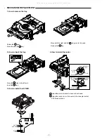
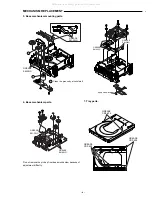
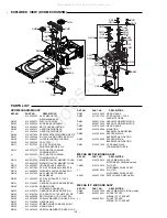
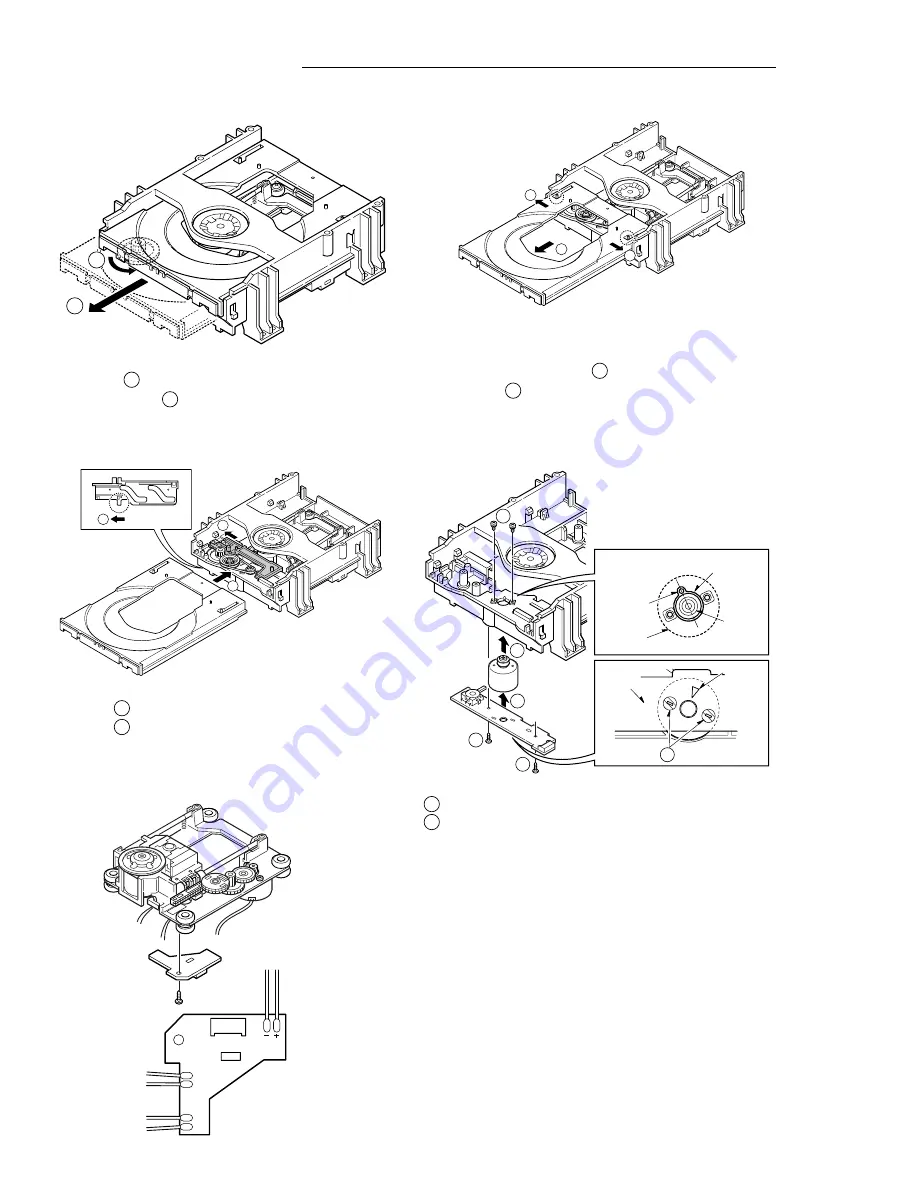
MECHANISM REPLACEMENT

4. How to install the motor.

1. How to remove the tray.

2. How to insert the tray.

1

2

1

1

2

1

1

2

Rotate the   1  gear.

Move forward the   2  tray.

Move both the right and left   1   tray pins to the ends.

Remove the  2  tray.

Move the  1  slide to the left end.

Insert the  2  tray.

4

4

3

5

1

2

ROUND

HOLE

MOTOR

PULLEY

SHASSIS

HOLE

TRIANGLE

MARK

SOLDERING

MECHA

P.W.B

1  Adjust the motor terminal to boss in the chassis.

3  Adjust the round hole of the motor to the triangle mark of

    P.W.B,and solder it.

CN002

SLED2

SLED1

GND
LMT SW

SP1-
SP1+

RED

BLACK

WHITE

ORANGE

BLACK

RED

3. How to install the IF PWB.

All manuals and user guides at all-guides.com

Summary of Contents for 137 118 04

Page 1: ...scription 17 Block diagram 32 Schematic Diagram DVD 34 Schematic Diagram MPEG and FRONT 36 Wiring Diagram DVD MPEG A side 38 Wiring Diagram DVD MPEG B side 40 Schematic Diagram POWER SUPPLY 42 Wiring Diagram POWER SUPPLY FRONT MECHA SW and MECHA IF rear REMOTE CONTROLLER RB SL25 NEXT PREV FWD SLOW REV SLOW PAUSE STEP PLAY REV FWD CLEAR SEARCH MODE 1 2 3 C 4 5 6 7 8 9 0 ENT SETUP MENU AUDIO RETURN ...

Page 2: ...omponent Video out Y 1 0 Vp p 75Ω PB 0 7 Vp p 75Ω PR 0 7 Vp p 75Ω AUDIO OUT L 2 V rms R 2 V rms Power requirements AC 110 240 V 50 60 Hz Power consumption 11 W Dimensions 360 W x 55 H x 250 D mm Weight 1 9 kg This is a basic specifications Specifications subject to change without notice Y R L PB PR AUDIO OUT VIDEO OUT COMPONENT VIDEO OUT OPT DIGITAL OUT VIDEO OUT SELECT S COMPONENT S VIDEO OUT CAU...

Page 3: ... resistivity will still remain at a level of 50 to 60 G but the mechanical robustness will weaken Do not place in a dusty location The entry and deposition of dirt into or on the pickup lens or moving section will cause malfunction or degradation DVD MECHANISM REPLACEMENT Connectors Do not connect or disconnect while power is on Connecting or disconnecting signal wires or the main power cord when ...

Page 4: ...the 2 tray Move the 1 slide to the left end Insert the 2 tray 4 4 3 5 1 2 ROUND HOLE MOTOR PULLEY SHASSIS HOLE TRIANGLE MARK SOLDERING MECHA P W B 1 Adjust the motor terminal to boss in the chassis 3 Adjust the round hole of the motor to the triangle mark of P W B and solder it CN002 SLED2 SLED1 GND LMT SW SP1 SP1 RED BLACK WHITE ORANGE BLACK RED 3 How to install the IF PWB All manuals and user gu...

Page 5: ... CDF 409 GREASE CDF 409 GREASE EM 30LG GREASE EM 30LG A Clean the groove by alcohol well A A GREASE EM 30LG GREASE EM 30LG Apply screw lock GREASE EM 30LG GREASE EM 30LG 5 Base mechanism mounting parts 6 Base mechanism parts 7 Tray parts MECHANISM REPLACEMENT All manuals and user guides at all guides com ...

Page 6: ...OADER N Check IC800 and peripheral circuit When AC IN LOADERMO TOR turn Chec k OPEN or SHORTat pin 29 26 27 and 24 32 of IC800 Is the voltage at pin 4 of IC850 about 1 8V Check IC850 and peripheral circuit N Y Check IC800 IC818 IC822 and peripheral circuite e Y N Is th e volt age at pi n31 and 32 of FL about 2 5V Is the voltage at pin 6 and 24 of IC about 5V Is the voltage at pi n15 of IC about 3 ...

Page 7: ...ptical modul and peripheral circuit N N Check IC851 and peripheral circ uit Y Check SPDIF CD signal line of IC130 and peripheral circuit Is there waveform at pin 3 and 16 of IC809 Check SPDIF SEL IC800 pin177 signal line Y N Is there waveform at pin 1 and 16 of IC809 Pin 6 of IC859 is LOW B C Y Pin 6 of IC859 is HIGH B C NO ANALOG AUDIOOUT ON PLAYBACK Is there AUDIO signal at pin 8 and 11 of IC871...

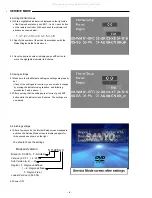
Page 8: ...on information are undefined In the following cases be sure to set up Market Region 1 When updating the system using CD R Part code 0PRADD7118 A 2 When replacing a DVD substrate While Market Region information are undefined the message Region Undefined is displayed on the screen NOTE Even if the condition is not under 1 or 2 above if the message Region Undefined is displayed be sure to set up Mark...

Page 9: ... a highlighted indicator is displayed on the right side of the Market denotation push numeric buttons on the remote controller When you push wrong number push CLEAR button The indicator reset to 00 Be sure to input by double figures For example in WM input 0 and 0 3 2 Specify the code of the model in accordance with the Market Region Setup Table above 3 3 Once the desired code is displayed push p ...

Page 10: ...perly set If any of the settings are incorrect you can make a change by moving the indicator using o button and following procedures 3 and 4 above 5 2 After ensuring that the settings are all correct push ENT button while the indicator is on Exit area The settings are now saved 6 Finishing settings 6 1 After a few seconds the Internal Setup screen disappears and then the Service Mode screen is dis...

Page 11: ... BOARD 1 Power on then open tray 2 It take on CD ROM for UPDATE software to the tray and tray close 3 Display UP DATE in the FL display 4 For the time being tray open and FL display remain UP DATE 5 When software loading finished UP DATE on a FL display disappears 6 Next set up market code and region code by SERVICE MODE CD ROM part code is 0PRADD7118 A CAUTION After an MAIN board 614 326 4279 or ...

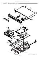
Page 12: ...INET CHASSIS 6 Y04 Y04 Y04 Y04 Y04 7 8 9 Y05 Y09 Y09 Y09 Y07 Y07 Y07 Y08 Y10 Y08 Y05 Y01 Y01 1 10 2 Y06 51 52 53 54 71 72 55 Y03 Y03 4 5 SL25 AU 3 This is a basic exploded view All manuals and user guides at all guides com ...

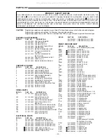
Page 13: ...11 021 6405 SCR S TPG BIN 3X8 DG PWB Y08 411 021 6405 SCR S TPG BIN 3X8 SHIELD FRONT Y09 411 021 3701 SCR S TPG BIN 3X10 ELECTRIC PART FIX ELECTRICAL PARTS REF NO PART NO DESCRIPTION 51 614 325 7639 ASSY WIRE LOADING DVD 52 645 057 3897 FLEXIBLE FLAT CABLE IF FFC or 645 057 8106 FLEXIBLE FLAT CABLE IF FFC 53 645 057 3880 FLEXIBLE FLAT CABLE PICK FFC or 645 057 8090 FLEXIBLE FLAT CABLE PICK FFC 54 ...

Page 14: ...301 645 048 3820 SWITCH PUSH or 614 220 5471 SWITCH TACT or 614 240 1002 SWITCH TACT or 645 006 5958 SWITCH PUSH 1P 1T S8400 645 043 7250 SWITCH SLIDE 2P 2TX4 SG841 645 055 3202 SURGE ABSORBER SG842 645 055 3202 SURGE ABSORBER SG871 645 055 3202 SURGE ABSORBER SG872 645 055 3202 SURGE ABSORBER X1500 645 017 0157 OSC CERAMIC 16 93MHZ X8230 645 053 4270 OSC CRYSTAL 27 000MHZ or 645 045 8293 OSC CRYS...

Page 15: ...2 082 6305 RESISTOR 68K J 1W S6040 645 048 3820 SWITCH PUSH or 614 220 5471 SWITCH TACT or 614 240 1002 SWITCH TACT or 645 006 5958 SWITCH PUSH 1P 1T S6041 645 048 3820 SWITCH PUSH or 614 220 5471 SWITCH TACT or 614 240 1002 SWITCH TACT or 645 006 5958 SWITCH PUSH 1P 1T S6042 645 048 3820 SWITCH PUSH or 614 220 5471 SWITCH TACT or 614 240 1002 SWITCH TACT or 645 006 5958 SWITCH PUSH 1P 1T S6043 64...

Page 16: ... TPG PAN PCS 1 7X4 5 RACK FIX DM21 614 310 2083 GEAR RACK MOVE PICKUP FREE DM22 614 310 6159 SPRING COMP FOR BACK RUSH RACK DM23 614 310 2076 GEAR RACK MOVE PICKUP FIX DM24 411 018 4704 SCR PAN PCS 1 7X5 LIMIT SW FIX DM25 645 040 9899 SWITCH MICRO 1P 2T LIMIT SW DM26 412 057 8304 SPECIAL WASHER FOR GEAR 2 FIX DM27 614 310 2069 GEAR GEAR 5 DM28 614 310 6142 SPRING COMP FOR BACK RUSH DM29 614 310 20...

Page 17: ...2P CN162 6P CN002 6P CN872 CN870 CN871 DVD MECHANISM MAIN P W B AC IN WR491 WR490 FU490 1A 125V POWER SUPPLY P W B WH DIGITAL OUT A V OUT S VIDEO OUT DVD PICKUP CN100 24P S VIDEO COMPONENT SW S8400 This is a basic wiring connection All manuals and user guides at all guides com ...

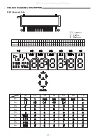
Page 18: ...0 21 22 23 24 25 26 27 28 29 30 31 32 F F NP NP 7G 6G 5G 4G 3G 2G 1G NC NCNCNCNCNCNCP9 P8 P7 P6 P5 P4 P3 P2 P1 NP NP F F ON G PIN NO CONNECTION Note F F Filament pin nG Grid pin Pn Anode pin NP No pin NC No connection 1G 2G 3G 4G 5G 6G 7G P1 P2 P3 P4 P5 P6 P7 P8 P9 All manuals and user guides at all guides com ...

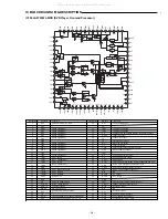
Page 19: ...t change RF servo signal gain up RF EQL band change TE output change WO output change Power supply Servo system Tracking hold H hold Tracking bottom band change High band Servo gain control RREC FE PP TE Terminal No 1 2 3 4 5 6 7 8 9 10 11 12 13 14 15 16 17 18 19 20 21 22 23 24 25 26 27 28 29 30 31 32 Symbole CAP VCC PDRF PD1 PD2 PD3 PD4 GND FIN1 FIN2 PIN1 PIN2 TIN1 TIN2 LDD1 LDS1 LDD2 LDS2 GND LD...

Page 20: ... X16MIO DVDCKIO VPDO VCOC VRFFR HDAT 7 0 HADR 12 0 HRDB HWRB HCSB HWAITB HIRQOB FDO TDO SLDO SPDO SGC TBAL FBAL BST FO TSTDO TSTDI TESIO HFLIO EMPH FSX EFLG DOUT LRSY ROMCK ROMXA C2F MRASIB MCASUB MCASLB MOEB MWEB MD 15 0 MA 12 0 AVACKO AVREQI AVDACK AVSCTB AVERRB AVD 7 0 A D Block D A Block Servo Block SLC Block 8 bits A D 8 bits D A Servo DSP 16x16 32 32 MPX RF I F Block FC Counter TR Counter EV...

Page 21: ...cy comparison filter connect Filter connect 1 Filter connect 2 Filter connect 3 Voltaji moniter Charge pump PCH control voltage Constant current charge pump current set of phase comparison Constant current charge pump current set of frequency comparison EFM playback PLL VCO oscillation renge set CD EFM playback PLL VCO oscillation range set DVD EFM PLL JV power supply Analog 3 3V Analog GND JV JV ...

Page 22: ...7 26 25 24 23 22 21 20 19 VIN1 B VIN2 VIN2 VIN2 VIN3 VIN3 VIN3 REG IN REG OUT VREF OUT CH1 VIN1 VREF SW VREF IN VIN4 VIN4 VIN4 MUTE VCONT S GND FWD REV VCC2 VL0 VL0 V04 V04 V03 V03 V02 V02 V01 V01 VCC1 VIN1 VIN1 A VIN1 A VIN1 B SIGNAL SYSTEM GND LOAD OUTPUT Voltage Setting MUTE BTL AMP OUTPUT ON OFF Thermal Shutdown O U T P U T VIN1 VREF SW 5VREG PNP Ext 22k 11k AMP B AMP A 22k 11k 22k 11k 22k 11k...

Page 23: ...3 Drain terminal Source terminal Ground terminal Overcurrent Feedback Latch trigger terminal MOSFET drain MOSFET source Ground Input of overcurrent detection signal constant voltage control signal latch circuit operation signal D S GND OCP F B Tri 5 4 Input of power supply for control circuit VIN Power Supply terminal Latch Delay Drive REG 5 Q K Internal Blas PWM Latch Icanl OVP TSD Tri All manual...

Page 24: ... software Use general interrupt I Controled general I O by microcomputer software Use general interrupt I SSC mode synchronization communication data reception Controled general I O by microcomputer software SSC mode synchronization communication data transmission Controled general I O by microcomputer software SSC made synchronization communication clock reception Controled general I O by microco...

Page 25: ...ltiplex digital video O CPUJTAG data O Probe UART data O Audio master clock I O 128 192 256 or 384fs sampling frequency Programable use S PDIF O N C Digital stereo audio serial data O Digital stereo audio serial data I Digital stereo audio bit clock O Palarity is programable Digital stereo audio LR clock O AOUT and AIN data output or latch clock trailing edge or last transition edge programable Co...

Page 26: ... by microcomputer software ATAPI PIO read signal O Controled general I O by microcomputer software ATAPI PIO ready signal I Survo DSP ready signal I Controled general I O by microcomputer software ATAPI data I O Controled general I O by microcomputer software ATAPI address signal O Controled general I O by microcomputer software ATAPI address signal O CD DSP error signal I Controled general I O by...

Page 27: ...g I SDRAM data I O SDRAM address O SDRAM low select O Active low SDRAM column select O Active low SDRAM clock O Same internnal process clock SDRAM data mask O Active high SDRAM bank select O SDRAM chip select O Active low SDRAM write enable O Active low External memory data I O External memory address O Used MEMAD 18 16 for PLL debug Externaal address O Controled general I O by microcomputer softw...

Page 28: ...IVALENT CIRCUIT Refer to BLOCK DIAGRAM FUNCTIONS GND Pin VDD Pin Voltage Detect Pin Capacitor Connect Pin with Delay Reset Signal Output Pin IC802 PST3627U System Reset IC851 PQ070XZ01Z Regulator 1 2 5 3 4 DC INPUT Vin ON OFF CONTROL Vc DC OUTPUT Vo OUTPUT VOLTAGE ADJUST Vadj EXCLUSIVE IC IC859 NC7SZ157P6 UHS 2 Input Non Inverting Multiplexer I1 GND I0 1 2 3 6 5 4 S Z Vcc Pin Name I0 I1 S Z Descri...

Page 29: ...CE OE WE BYTE RY BY WP RESET VDD VSS Pin Name Bank Selective Address Flush Bank Address Flush Bank Block Address Flush Bank Sector Sddress Data Input Output Chip Enable Output Enable Write Enable Bait Pin Ladey Beje Output Write Protect Reset Power Supply Ground Functions Selects bank 1 when L and bank 2 Sapply address for flush bank Select flush bank for erease Select flush bank sector for erease...

Page 30: ...es data output Hi Z ISHZ sfter the clock and masks the output Blocks data input when L U DQM active Data inputs outputs are multiplexed on the same pins Power and ground for the input buffers and the core logic Isolated power supply and ground for the output buffers to provide improved noise immunity This pin is recommended to be left No Connection on the device Pin CLK CS CKE A0 A10 AP BA RAS CAS...

Page 31: ...ignored Key Data Input Pins The data sent to these pins are latched at the end of the display cycle Logic Ground Pin Logic Power Supply High Voltage Segment Output Pins Also acts as the Key Souree Pull Down Level High voltage Segment Grid Output Pins High Voltage Grid Output Pins Oscillator Input Pin A resistor is connected to this pin to determine the oscillation frequency Data Output Pin N Chann...

Page 32: ...dio Data Input DSD Input Mode Lch DSD Bit Stream Input Audio Data Bit Clock Input Master Clock Input Infinite ZERO Detect Flag Digital GND Digital VDD Rch DAC Output Analog GND Analog VDD Lch DAC Output Mid Rail Decoupling Point Reference N Side For DAC Reference P Side For DAC Software Mode Chip Select Pin 3 Ways Input Hardware Mode Word Length Decision Pin Input Data Control Mode Switching Pin L...

Page 33: ...PDIF DVD 3 3V 3 3V 3 3V FD TD SLD 9V 3 3V RF5 12V 5V 3 3V 1 8V 9V FL2 FL1 30V 12V 9V 5 6V DAC_A DAC_B DAC_C COMPOSITE DAC_D L CH R CH AMUTE SPDIF L CH R CH SPDIF MD MD LD LD RF5 3 3V SPDIF CD SPDIF DVD SPDIF SEL 30V 12V 9V 9V 5 6V 3 3V 1 8V PD 3 3V 2 5V SPD SP SP FOST TOST FOST TOST DVD_ CD DVD_ CD LDON1 LDON2 SGC DEFECTO FC BST TBAL FBAL XHTR TEC ADRREC ADBH ADTE ADFE RFP RFN ADPH BHC WO FD TD SL...

Page 34: ...IO LDON2 LDON1 XHTR WRQ DEFECTO DVD_ CD C1846 INT_DEC RDY LSI_RST RD WR CS_DVD GUP C1090 R1091 X1500 CN162 C1320 RN100 RN101 22K 47 25 27K 15K 10K 0 1 0 1 10K LA6560 10K 10K 10K 10K 12K 0 1 4 7K 4 7K 0 1 100 100 100 4 7K 1000P 1K 18 KTA1505 10 50 10 50 KTA1505 1K 1000P 1000 18 000 KTC3875 3 3K 4 7K 10K KTC3875 10K 10K 0 1 0 1 0 1 000 KTC3875 KTC3875 18 18 1 0 1 220 6 8K 330 0 1 150 6 3 000 0 1 100...

Page 35: ...1ET 70 0 1 1000 0 1 0 1 0 1 0 1 0 1 0 1 0 1 0 1 0 1 0 1 0 1 0 1 0 1 0 1 0 1 47 25 PST3627UR 0 01 0 1 100P 4 7K 120 27 000MHz 18P 18P 390 33 33 33 33 33 4 7K 4 7K 4 7K 0 1 0 1 0 1 0 1 0 1 0 1 4 7K 4 7K 4 7K 4 7K 4 7K 470P 4 7K 0 1 4 7K 4 7K 0 1 4 7K 4 7K 1SS355 100K 0 1 KDS226 47 25 470 KTA1504 100 16 100K 100 0 1 NC7SZ157 XH04 4 7K 4 7K 4 7K 4 7K XH04 4 7K 4 7K PQ2L2182MSP 0 01 47 25 0 1 02 1K 0 1...

Page 36: ...0 R8883 3 8 R 8 88 R8 R R 8 R88 R 88 R 88 R8884 84 8 R 8 88 R8 R8 R 8 R88 R8 R 88 R 88 R8885 85 R R 8 88 8 R R 8 R 8 R R R R R 88 R 88 R 88 R C8882 2 C8882 8 C 8 88 C8 C88 C C8 C88 88 C C 88 L8582 2 8 L 82 82 L L85 58 L8 L858 58 L8 8 8 L L C8584 C8584 C 8 C 8 58 C85 C C 85 C 58 C C 58 R8603 03 03 R 0 603 3 R8 R R 6 R86 R R 60 R 60 R8019 R 019 9 1 R 1 01 R8 R 0 R80 R 0 R 0 R 0 R8604 04 604 860 0 60...

Page 37: ...AGRAM DVD MPEG B SIDE 1AD4B10D1700AA 5V DGND AGND VGND VGND AGND DGND DGND AGND VGND DGND DGND 3 3V DGND DGND DGND AGND DGND AGND AGND DGND AGND RF5 DGND DGND DGND SL25 AU All manuals and user guides at all guides com ...

Page 38: ... DSK10E DSK10E DSK10E SB140 1000 6 3 0 01 10 50 MTZJ12B 0 01 2 2K KTC3203 1SS133 BSKIP FSKIP 1SS133 STOP 1SS133 PLAY POWER 6 8 1SS133 1SS133 12 33K 0 1 56K 56K 56K 56K RGP02 15 0 022 400 STR G6351 630 750 H11A817B 3 2 1 1 2 3 4 5 6 1 2 3 4 5 6 7 8 9 10 11 12 1 2 3 4 5 5 6V 12V 9V FL2 FL1 30V 12V 9V 5 6V FL1 FL2 30V 1AD4B10D1821A BL 1 3 6 5 7 8 9 10 12 13 14 4 2 11 TO DVD PWB TO DVD PWB BW SL25 AU ...

Page 39: ... CON RF GND D GND D GND D GND 9V 5 6V AV GND 12V D4802 D4803 D4809 D4805 PR482 D4806 PR481 PC490 PT490 IC490 J4818 PR484 R4806 C4811 C4807 FU490 C4907 R4908 L4900 D4906 D4900 J4817 D4904 D4905 C4904 R4900 D4902 C4900 R4913 R4914 R4915 R4905 R4904 C4908 D4910 C4902 R4912 R4910 R4901 R4911 C4822 L4801 C4815 C4812 R4903 C4910 R4810 R4809 R4805 IC483 R4802 C4905 R4916 Q4820 C4801 C4821 J4820 J4821 D49...

Reviews: