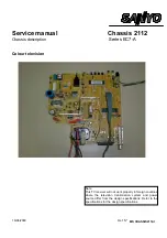
Service manual
CHASSIS 2112-Series EC7-A
7
important mark off that the good functioning of current control depends on the state of R811 and R812, which can
be altered in case of failure of Q800.
Therefore,
whenever the transistor is replaced by failure, new resistances must change R811and R812
.
The regulation in voltage is made by means of the comparison of the signal in pin 14 (" VOLT_FEEDBACK ") with
an internal reference of 2.5 volts. This comparator output is the goal for the current control. In addition, it is also
connected at pin 13 ("E/A_OUT") in order to perform the frequency compensation of the feedback loop. Voltage at
pin 14 comes from rectification (D804, C806) of the transformer primary output, by means of a voltage divider and
the adjustment potentiometer VR800.
This maintains 2,5 volts at pin 14, therefore the power supply controlled output is the primary one (to a voltage that
depends on VR800), remaining the other outputs only regulated by transformer ratio.
4.1.3 "Stand-by".
MC44603P has a stand-by mode based on the primary peak current measurement. If it does not arrive to certain
level (programmable with R812), it switches to work at a fixed frequency of around 18 kHz (controlled by R813).
The R812 value is chose by design to assure that when the TV goes to stand-by mode also the IC800 goes to this
mode.
4.1.4
“+8v” and “+5v” regulators
4.1.4.1 Configuration.
They are lineal regulators that are disabled in stand-by mode. The configuration of the “+8v” has a differential
amplifier configuration (Q859 and Q860) with Q853 as a transistor that drives the signal. The “+5V” (Q856 and
Q857) has an emitter follower configuration. Both regulators use the “+5V_M” voltage (from IC850 [7805]) as a
reference.
4.1.4.2
“stand-by” / ”ON” control
This control is done by means of the following signals and components chain: “ON” signal from the micro (activated
at high level), Q852, Q851 (B1_L), “+8V” polarisation (R869) and “+5V” polarisation.
In order to achieve a correct IC400 (line oscillator) start-up is necessary that the “+8V” raises in ramp about 100ms.
This is obtained with the integrator that Q850, and the circuitry associated to its base, forms with the “+8V”
regulator. The weak load of the decouplings that there are in " +8V " also avoids a peak of discharge in B2 at the
moment when the regulator switches on, because a peak in this point can activate the micro reset (Q858) and force
the “ON” signal to a low level. In this case an on/off sequence will start, it is possible to detect it visually because the
LED will be blinking each second approximately (it is not the ERROR_1 indication. When the micro indicates
ERROR_1 the time between sparkles will be longer).
4.1.4.3
Regulator output short circuit protection.
The chain described above allows the microprocessor knows if there is a short circuit at any output regulators. The
microprocessor has to watch the “-SUP_FAIL”, so if “-SUP_FAIL” signal is at low level when the TV switches ON
then the microprocessor deactivates the “ON” signal and the regulators will be also disabled. In this case the micro
will indicate ERROR_4. But there is another possibility, the B2 supply can decrease enough to activate the
microprocessor reset and the TV set will start the on/off sequence (explained before).
4.1.4.4
Mains switch off detection.
When the TV set is switched off, while C803 (primary electrolytic) is discharging, the microprocessor has to activate
the speaker mute (to avoid the “pop” noise) and discharge the CRT. The C803 discharge is detected by means of
secondary B2 winding because of the negative voltage of supply commutation pulses (this voltage reflexes,
depending on the turn ratio, the primary voltage rectified). The used circuit to detect the switch off situation and
generate the “-PD” signal for the microprocessor is Q855 and its periphery (negative level detection, filtering and
comparison with a reference level).
Summary of Contents for CE14A2-C
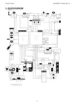
Page 20: ...Service manual CHASSIS 2112 Series EC7 A 5 3 BLOCK DIAGRAM ...
Page 48: ......

