-6-
F7YLV
Y
U
V
HD
VD
IC7207
FIELD
MEMORY-1
IC7206
FIELD
MEMORY-2
IC7205
SCAN
CONVERTER
<SAA4991WP>
IC7201
A/D, D/A
TIMING
CONTROLLER
<SAA4977H>
PLL
VCO
Y/U/V
SWC
SWCK
SRCK
SRCK
LLD
2Y_out
2U_out
2V_out
2HD_out
2VD_out
IC7208
IC7203
IC7202,IC7204
26
28
30
22
20
79
76
74
71
70
72
15
26
62
26
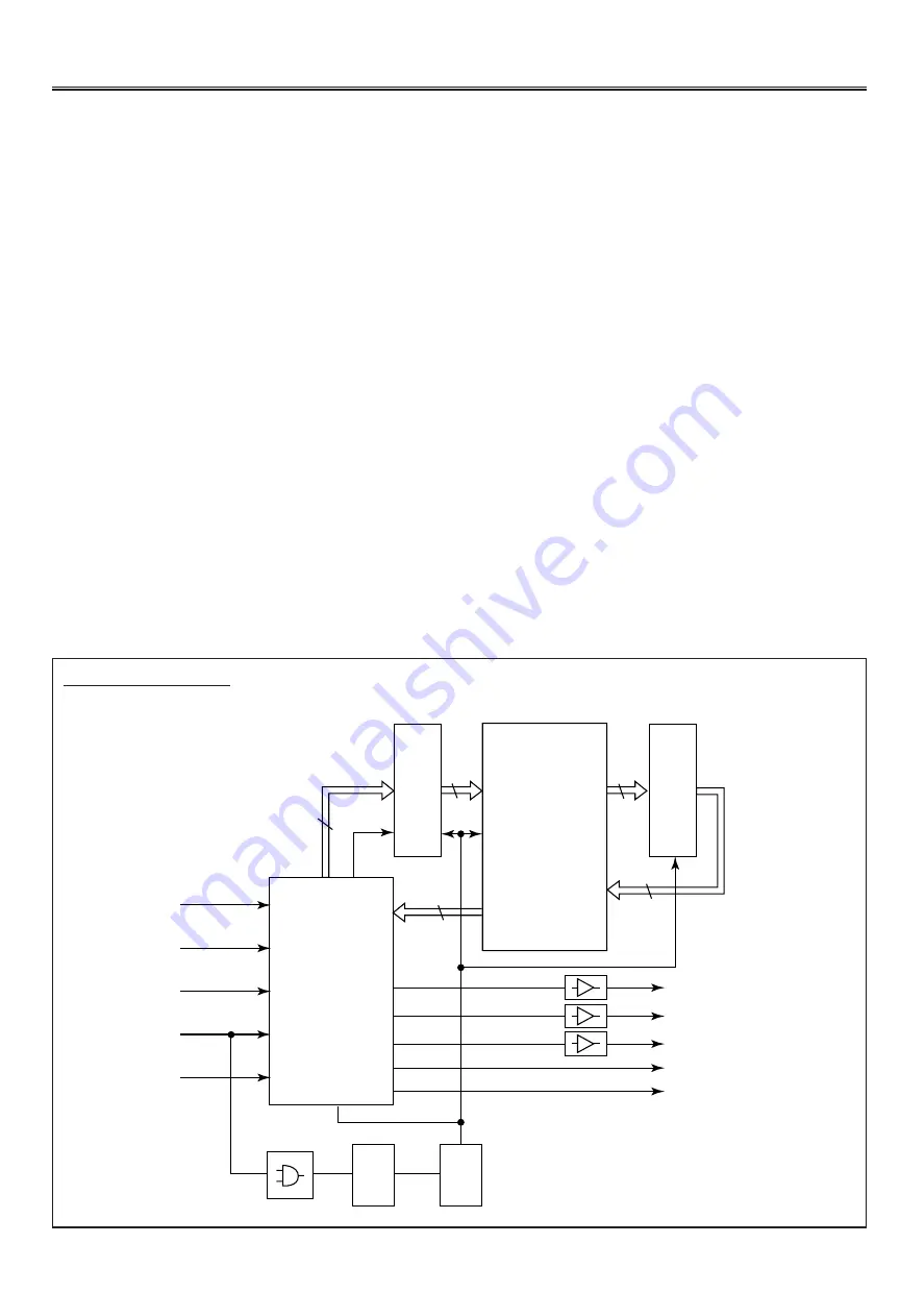
Digital scan circuit
100Hz Digital Scan Converter circuit
100Hz converter circuit consists of the following ICs.
- SAA4977H
A/D, D/A, Timing generator
- SAA4991WP
100Hz converting processor
- SAA4955TJ x2
1.9Mbit field memory
-MC74HC4046AF
PLL(Phase Locked Loop)
The Y/U/V signals decoded in the HOP IC (IC101) are sent to the scan converter circuit. The
Y/U/V signals are sent to SAA4977H through the AC coupling capacitors and converted to 8bit
digital data with 16MHz sampling clock at the A/D converting stage in the IC respectively.
SAA4977H has built-in L.P.F. and the input stage for A/D conversion, so no external L.P.F. are
required. The digitalised U/V signals are compressed with 1 by 4 at SAA4977H and sent to the
field memory IC, SAA4955T as the 8bit Y-signal and 4bit C-signal data stream. Two fields picture
information are always maintained by two field memory IC, SAA4955TJ.
SAA4991WP creates a 100Hz converted field picture information to display next field from these 2
field picture information, and sends this to SAA4977H. There are two ways to create a new field
picture information, the one is creating the compensation data by detecting the motion image in
DIGITAL SCAN OPERATION
Fig.-7
Summary of Contents for CE32WH3-F
Page 35: ... 35 F7YLV 17 20 21 5 19 2 16 15 18 4 11 ...
Page 68: ...MAIN BOARD CIRCUIT SIDE MAIN BOARD COMPONENT SIDE ...
Page 79: ......


