background image

-11-

N4JK

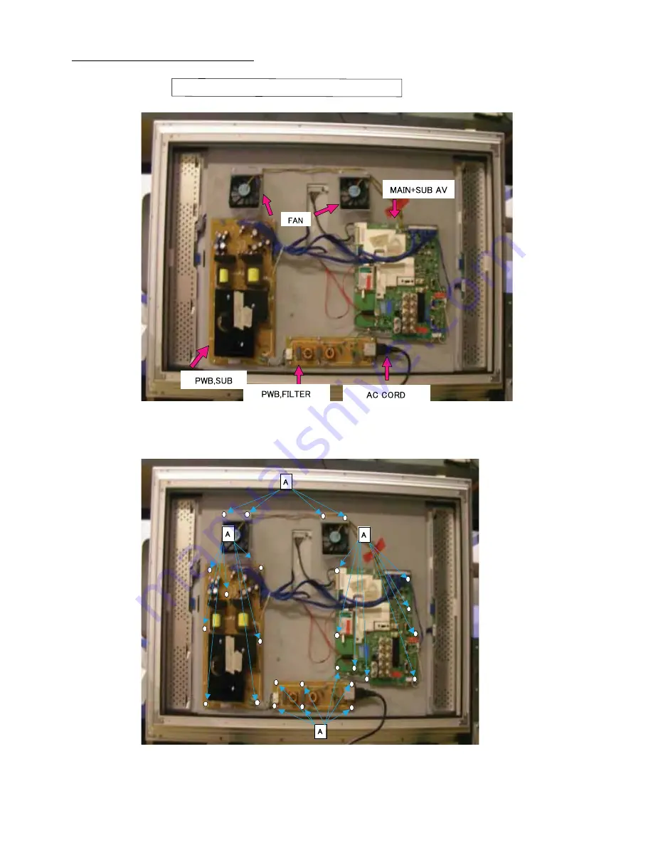
Mechanical Disassembly contd.

Location if Circuit Board and Electric Parts

Note: Control Board is fixed on Cabinet Front.

3. Chassis and Fan Removal

Screw A : M3 x 6

Summary of Contents for CE42LM4WPR-E

Page 1: ... the design specifications Contents Safety precautions Specifications 2 Service Mode Service Data 3 7 HDMI PC Component Signal Support Timing List 8 Mechanical Disassembly 9 12 Block Diagram 13 Power Diagram 14 Power and Control Diagram 15 RS232 Settings 16 17 Troubleshooting 18 IC Descriptions 19 20 IC Block Diagrams 21 22 Cabinet Parts List 28 Pin description of semiconductors 29 Electric Parts ...

Page 2: ...system PAL NTSC4 43 PAL NTSC4 43 NTSC3 58 IN AV MODE Receiving channel UHF 21 69 VHF E2 E12 F2 F10 R1 R12 CATV X Y S1 S41 B Q Aerial input impedance 75ohm AV terminal AV1 CENELEC standard INPUT Composite video RGB and Audio L R OUTPUT TV output with composite video and audio L R AV2 BNC INPUT RGB H and V Y Pb Pr and audio L R OUTPUT RGB H and V Y Pb Pr AV3 BNC INPUT Composite video OUTPUT Composit...

Page 3: ...same time alternatively From Hotel Mode press and hold the green button on the remote control for 3 seconds To select the service item and change data value To select the adjustment item use the 5 or 6 buttons To change the service data use the Volume LEFT or Volume RIGHT buttons The data which is set in the service mode is stored into the memory IC automatically EXAMPLE 000 UK4B 07 45 ITEM NO SEC...

Page 4: ... 4 N4JK SERVICE DATA ...

Page 5: ... 5 N4JK SERVICE DATA contd 1 ...

Page 6: ... 6 N4JK SERVICE DATA contd 2 ...

Page 7: ... 7 N4JK SERVICE DATA contd 3 ...

Page 8: ...1 74 92 XGA 1024 _76 8 61 00 75 70 XGA 1024 _76 8 60 24 75 08 MAC_Normal 19 1280 _96 0 60 00 60 00 SXGA VESA 60Hz 1280 _10 24 79 976 75 025 SXGA VESA 75Hz 1280 _10 24 62 50 58 60 SXGA 1280 _10 24 63 370 60 01 SXGA 1280 _10 24 63 34 59 98 SXGA 1280 _10 24 63 74 60 01 SXGA 1280 _10 24 63 79 60 18 SXGA 1280 _10 24 63 90 60 00 SXGA 1280 _10 24 71 69 67 19 SXGA 1280 _10 24 76 97 72 00 SXGA 1280 _10 24 ...

Page 9: ...have already disassembled the set This makes the warranty regarding this IP model invalid After finishing the service make the set tamper proof again with silver paint 2 Rear Plate Removal Remove screws A 6 pcs then remove the Terminal Cover Fig 2 Remove screws B 4 pcs then remove the AV Terminal Fig 3 Remove screws D 20 pcs Fig 6 Remove screw C Fig 5 then remove the Rear Plate ...

Page 10: ... 10 N4JK Mechanical Disassembly contd ...

Page 11: ... 11 N4JK Mechanical Disassembly contd Location if Circuit Board and Electric Parts Note Control Board is fixed on Cabinet Front 3 Chassis and Fan Removal Screw A M3 x 6 ...

Page 12: ... from the Main Board 2 Remove the lead wire of the inverter from the Power Board Main Board 3 Remove the LVDS cable from the LCD Panel 4 Remove cables from the Inverter area or Power and Main Board 5 Remove screw A 20 pcs 6 Remove the Cabinet Back Mechanical Disassembly contd ...

Page 13: ...SWITCH RGB YPBPR VIFIN1 LOC2 PANEL LVDS VIF TUNER GTV SCART1 CVBS1 TV OUT CVBS RGB1 CVBS3 RGB SWITCH VIDEO SWITCH BA7652 SVO6 CVBS6 CVBS CVBS_Y4 CVBS_Y5 SWO1_CVBS20_Y20 CVBS30_Y30 DVBO_IFVO_FMRO HDMI TMDS BA7603 SiI9021 HDMI DECODER D RGB RGB CVBS PV10_23 IN_R IN_G IN_B R3_PR31 G3_Y31 B3_PB31 PC RGB RGB SWITCH BA7657 MATRIX COMPONENT YPBPR RGB H V Y G Pb B H V Pr R H V OUT IN OUT IN Outline ...

Page 14: ...10 IC6609 IC6608 IC6607 IC6606 IC6605 IC6603 IC6602 13V_PWR 9V 12V_FAN 5V_SW 3V3_SW D5V D3V3 1V8_SW D1V8 POWER ARCHITECTURE D6601 D6621 D6618 D6616 D6607 D6606 D6605 D6604 D6615 D6614 TO IC801 PIN E10 5V 1 2 3 4 5 KQ 24V 6V D3V3 D5V 3V3_SW 5V_SW 12V_FAN 9V PROTECT ARCHITECTURE 2 3 4 5 KR POWER TO UNIT POWER DIAGRAM FOR UK4B ...

Page 15: ...1 8 1 5 12V 5V 3 3V K3000 cct K3A 12V K3003 K603 K303 03 K3Q K3R KR 5V S B K605 K3002 K605 02 5V gnd 16V 12V Gnd Gnd Gnd Gnd NC NC NC NC 1 2 3 4 5 6 7 8 9 10 11 12 13 14 1 2 3 4 5 6 7 8 9 10 11 12 1 2 3 4 5 6 7 8 9 10 11 12 1 2 3 4 5 6 7 8 9 10 11 12 13 14 5V S By Gnd D5V Power on ON OFF VBR NC NC NC NC Gnd Gnd K3001 NC NC NC NC NC 1 11 1 6 POWER_3 BL_ADJ BL_ON 3 3V S B KP R1600 R1601 gnd 1AA0B10H...

Page 16: ... used for operating multiple monitor sets from a single pc via the RS232 command line If you set your monitor address to 000 it will never respond to any addressing command from the pc If the address from the pc is FFF all monitor sets will execute the command The address format command is defined by one command one line which starts with A and ends with carriage return 0x0D An address is added at...

Page 17: ...de Title in 16 9 direct Wide Zoom 14 9 direct Wide Title in 14 9 direct RGB direct AV2 RGBHV direct AV2 YPbPr direct AV3 direct HDMI direct PC direct PC Auto adjust Factory settings Power save ON Power save OFF Child lock ON Child lock OFF RC inhibition OFF RC inhibition ON Status Read Command Table Command Item Note _means No Function C Panel operating time CR0 CR1 CR WIDE CR PICTURE CR SIGNAL CR...

Page 18: ...ible line on the picture Part of the display is poor No working of RC handset No working or the front key Switch After indication of the display then 30 seconds later come into standby Change the FAN Change the FRONT board Change the RC or FRONT board Change the panel Change the COMP board If not change the panel Change the LCD panel Check to voltage of KR 3 5V Change the power board Check the fus...

Page 19: ...e for internal loss in the YPbPr RGB HV loop IC2006 RS232 to 5v decoder encoder It converts the RS232 signal from K2008 into a TTL signal that can be understood by the CPU IC2010 IC2007 8 11 5v to 3 3v logic conversion for the CPU IC2010 IC2009 Reset pulse generator for the CPU IC2010 IC2010 CPU with internal program flash memory The software version programmed into this device can be found in the...

Page 20: ...rtor HDMI data from K1006 is fed into this IC The IC then extracts the video and audio in digital format and sends the data to IC801 Audio data is converted to analogue via IC8501 IC801 This IC is the main control IC for the entire TV It incorporates 1 CPU for control and on screen graphics presentation 2 Video signal processor for controlling picture presentation and quality 3 LCD scaler for conv...

Page 21: ... 3D COMB FILTER RDS CVBS Y U V DEINTER LACER NOISE REDUCT BLACK STRETCH WHITE STRETCH HORIZ SCALER PEAKING LTI CTI COLOR FEATURES YUV TO RGB MATRIX ADC STEREO SOUND DECODER AUDIO IN OUT LINE O I C S C SW I2S HP OUT LS OUT MEMORY INTERFACE CNTRL ADDR DATA 6 12 16 16 MBit SDRAM 8051 MICRO CONTR TXT DECODER OSD OSD BLENDER I Os 24 RGB YUV alpha OUTPUT FORMAT RGB DACs RGB ITU H V CLK ClkRef 4 30 10 RO...

Page 22: ... 22 N4JK IC BLOCK DIAGRAMS IC1205 BA7603F IC151 BA2904 1 2 3 4 5 6 7 8 CH1 CH2 _ _ VCC OUT2 IN2 IN2 OUT1 IN1 IN1 VEE ...

Page 23: ... BIAS SCL SDA ADR MUTE GND LOUT1 0dB V CC ROUT1 0dB LOUT2 0dB ROUT2 0dB LOUT3 0dB ROUT3 0dB BIAS Logic 33 35 1 3 5 7 9 11 13 15 17 34 36 2 4 6 8 10 12 14 16 18 19 23 22 21 20 24 30 29 28 27 26 25 31 32 IC2002 TSH3441 Top View OUT2 1 IN2 OUT1 Vcc 2 3 7 8 OUT3 IN1 4 6 IN3 GND SO8 Pin1 identification 5 6dB 6dB 6dB ...

Page 24: ... 24 N4JK IC BLOCK DIAGRAMS IC2003 TC7WH125 IC2006 SP3232 V 1 2 3 4 13 14 15 16 5 6 7 12 11 10 C1 V C1 C2 C2 R1IN R2IN GND VCC T1OUT T2IN 8 9 SP3232E T1IN R1OUT R2OUT T2OUT IC2007 IC2008 IC2011 TC7SET08 ...

Page 25: ... CC CNV SS P1 7 INT 1 CNTR 0 P16 CLK0 P15 RxD0 P14 TxD0 P3 7 TxD 10 RxD 1 P3 0 CNTR 0 CMP1 0 P3 3 INT 3 P3 1 TZ OUT CMP1 1 P3 2 INT 2 CNTR 1 CMP1 2 IV CC 3 AV SS AV CC V REF P03 AN4 P02 AN5 P01 AN6 P00 AN7 TxD11 P06 AN1 P05 AN2 P04 AN3 P45 INT0 P10 KI0 AN8 CMP00 P11 KI1 AN9 CMP01 P12 KI2 AN10 CMP02 P13 KI3 AN11 P0 7 AN 0 MODE TC IN IC2012 BA50BC0FP Vref TSD 0CP _ Driver R1 R2 Vcc 1 PIN N C 2 PIN O...

Page 26: ...K DIAGRAMS IC6600 IC6604 LA5754MP DL E Y Decoder I O Buffers and Data Latches Address Buffers Latches X Decoder DQ7 DQ0 Memory Address OE CE WE SuperFlash Memory Control Logic Functional Block Diagram IC4001 ST39VF0200 ...

Page 27: ... O1 I O2 I O3 I O4 I O5 I O6 I O7 SU01783 NOTE ALL I Os ARE SET TO INPUTS AT RESET Vcc INT LP FILTER PCA9534 IC601 L6562D MULTIPLIER AND VREF2 OVERVOLTAGE DETECTION VOLTAGE REGULATOR UVLO INTERNAL SUPPLY 7V 2 5V R1 R2 R S Q DRIVER STARTER ZERO CURRENT DISABLE 2 1 V 1 6 V Vcc 8 1 2 3 4 ZCD Vcc INV COMP MULT CS GD 7 5 GND 6 25 V 40K 5pF 15 V Starter stop DETECTOR THD OPTIMIZER ...

Page 28: ... Description Item Part No Description CE42LM4WPR E 00 CABINET PARTS 1 665 000 8618 ASSY REAR PLATE N4JK 2 665 000 7307 REAR PLATE GASKET N4JK 3 665 000 7642 5G SACHET SILICA GEL 4 412 075 4003 SPECIAL SCREW 4 2X9 5 5 412 075 4409 SPECIAL WASHER N2MJW ACCESSORIES 6 645 079 4421 ASSY REMOCON JXPLA WEEE 665 000 9325 INST MANUAL N4JK 1 665 000 8632 INSTALL INST SHEET N4JK 1 2 3 4 5 ...

Page 29: ...K A K A C B E C B E C B E 1 2 3 4 5 6 Index 1 2 N Index Index 1 2 N 2 1 3 IN OUT GND 2 1 4 2 1 3 Index 1 N Index 1 N Index 1 N Index 1 N Index 1 N Index 1 N 2 1 3 1 2 3 2 1 3 RESET GND Vdd 5 3 D G S D G S K Cathode A Anode C Collector B Base E Emitter D Drain G Gate S Source Diode Transistor FET IC E1 C2 E2 C1 B2 B1 Index Diode Transistor FET IC FET ...

Page 30: ...C CORD UK 665 000 6768 CORD POWER AC CORD AUS 665 000 8687 CORD POWER W900 665 000 8342 CORD POWER N4JK 665 000 8724 ASSY PLUG WP AC CON MALE 665 000 6775 ASSY PLUG WP AC CON FEMALE OTHER COMPONENTS ELECT BP EARTH 665 000 7802 NONSTANDARD WIRE ASSY KK 1 645 040 3002 FERRITE RING FIXING PIN KLP PN 665 000 7796 NONSTANDARD WIRE ASSY LVDS CABLE K602 1 645 020 3640 FERRITE RING also used in locations ...

Page 31: ... 31 N4JK ...

Page 32: ... 32 N4JK Sanyo Industries UK Ltd Printed in UK ...

Reviews: