background image

-15-

Service Mode Adjustments

A30C5

J472

J473

C471

R484

T471-H10

T471-H8

T471-H6

T471-H7

T471-H5

T471

J474

R481

MAIN BOARD

SCREEN VR
(Under side)

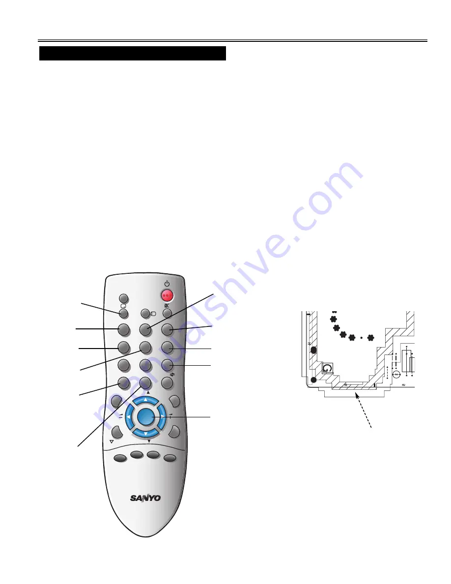
(1) Receive a monochrome circular pattern. 
(2) Set the brightness and colour to normal, contrast to maximum.
(3) Enter to the service mode. 
(4) Select No. 30 RBIAS (Red Bias), No, 31 GBIAS (Green Bias), and No. 32 BBIAS (Blue Bias) and set each data to 0

by pressing the or - key.

(5) Select No. 33 RDRIV (Red Drive) and No. 35 BDRIV (Blue Drive) and set each data to 64 by pressing the VOLUME

+ or - key.

(6) Turn Screen Control on the FBT (T471) to minimum (fully counter-clock-wise).
(7) Select No. 36 (1-line appear). 
(8) Advance Screen Control clockwise to obtain just  visible one colour line. If line does not appear, place this control to

maximum (fully clockwise).

(9) Raise each Bias Level with 1, 2, 5, 6, 9 and 0 keys to obtain just visible white line.
(10) Select No. 37 DRV (Drive Adjustments).
(11) Adjust Red and Blue Drive Levels alternately with 3, 4,  -/--  or RECALL key to produce normal black and white 

picture in highlight areas.

(12) Check for proper grayscale at all brightness levels. To turn off the TV Service Menu display, press the MENU key.

Note: 

If the Grayscale adjustment is made after picture tube replacement, check the High Voltage

Items 30-33, 35-37 GREY SCALE

1

2

3

4

5

6

7

8

9

0

TV/AV

TIMER

x

-/--

SWAP

CH SCAN

MENU

BASS

SOUND

S. SYS

SURROUND

PICTURE

CH

CH

A B

.

P

P

JXPSG

Red Bias -

Red Bias +

Green Bias -

Green Bias +

Blue Bias -

Blue Bias +

Press the

MENU 

button to exit

from service mode.

Red Drive -

Red Drive +

Blue Drive -

Blue Drive +

SM_29-BE8V(FC6-B)AUS  5/10/08  7:49 AM  Page 15

Summary of Contents for CP29YS2B

Page 1: ... 5A AUS 1 11 NZ UHF 21 69 A14 A69 J13 J62 28 69 AUS CATV S1 S41 X Y Z Z 1 Z 2 Video IF 38 0MHz Aerial Input Impedance 75Ω Ext Terminals Video inputs Phono jack x 2 1Vp p 75Ω DVD Input Component Video Jack Y 1 1 0Vp p impedance 75Ω Component Video Jack CB CR 1 0 7Vp p impedance 75Ω Audio inputs Phono jack L R x 2 436mVrms more than 40KΩ Video monitor outputs Phono jack x 1 1Vp p 75Ω Audio monitor o...

Page 2: ...without danger of electrical shock X RADIATION PRECAUTION The primary source of X RADIATION in television receiver is the picture tube The picture tube is specially con structed to limit X RADIATION emissions For continued X RADIATION protection the replacement tube must be the same type as the original including suffix letter Excessive high voltage may produce potentially hazardous X RADIATION To...

Page 3: ... 16V 13V 9V 9V 5V 36V FBT TUNER HORIZ DEF VERT DEF MAIN SOUND AMP SURROUND AV SW AUDIO CTL 1 CHIP IC CPU EEPROM POWER SUPPLY CIRCUIT D1910 LED A1901A RC RECEIVER FRONT CONTROL KEYS SW1901 SW1906 POWER ON OFF RC IN KEY IN Q111 IF AMP K1102 HEADPHONE JACK L OUT R OUT VIDEO MONITOR OUT AUDIO MONITOR OUT LEFT CR IN CB IN Y IN WOOFER OUT S TERMINAL HEATER R B G CRT UNIT VERT OUT HORIZ OUT R OUT G OUT B...

Page 4: ...D RED OUT Active High OSD GREEN OUT Active High OSD BLUE OUT Active High CRT UNIT POWER PROTECT IN POWER ERROR LOW POWER CIRCUIT etc IIC SCL IIC SDA IC801 MEMORY OSC X801 32 768KHz CPU OSC OUT CPU OSC IN LED ON TIMER LED OUT ON TIMER ON Low RC SIGNAL IN ACTIVE HIGH RC PRE AMP 30 SOUND MUTE MUTE H IC001 AUDIO AMP A101 F S TUNER RESET INPUT RESET LOW 40 5 6 5 4 IC3701 AUDIO CONTROL 19 20 S VIDEO IN ...

Page 5: ...VIDEO DET SOUND DET LIM AMP BPF 500K DET BPF FM DET FM AMP SW DC VOL 18P 15P 510K 0 01U 100U VDD AN4 P04 AN5 P05 AN6 P06 AN7 P07 150K 0 33U 2 2U 100 0 033U CPU GND 0 01U 100 100U 20K FBP 0 1U YC C YC Y 1U 1U 750 1U DVD Y CB 0 1U 4 43M 0 1U CR SVO FSC 0 047U 0 47U 12K 1U 0 01U 100U EXT V VCC 5V VCD INT V VCC OUT VIDEO RF AGC IF IN 1U 680K 2 2U 560 0 47U 47K 47K 0 1U SAW FIL 64 63 62 61 60 59 58 57 ...

Page 6: ... IN1 IN2 IN2 MODE SVR STANDBY MUTE LOGIC VCC 20 kΩ 20 kΩ 2 15 GND1 GND2 SHORT CIRCUIT AND TEMPERATURE PROTECTION N C N C N C TDA8944J IC501 Vertical Output LA78141 E THERMAL PROTECTION PUMP UP AMP N C Ver Output Output Stage Vcc Non Inv Input Inverting Input Vcc Pump Up Output LA7846N GND N C N C 1 2 3 4 5 7 6 8 9 10 ...

Page 7: ...M2 29 ON TIMER LED OUT On timer led out function 30 MUTE OUT Mute out function 31 IIC SDA1 IIC Bus Data Line 32 IIC SCK1 IIC Bus Clock Line 33 X tal Crystal Oscillator 34 X tal Crystal Oscillator 35 5V Supply 5V 36 Power Out Power On Off signal output 37 Bass Expander Bass Expander On Off function ON OFF OUT 38 VIF M OUT VIF M Out Bilingual Out function Bilingual Out 39 AD KEY IN Key signal input ...

Page 8: ...e second The CPU detects that this has occurred and outputs the signal from pin 36 to switch off the power supply lines Releasing the protective circuit and restoring power supply To release the protective circuit and restore power supply turn the power to the TV set OFF and then ON again via either the main power switch or the ON OFF button on the remote control This will work only if the power s...

Page 9: ... TV set while the above On Screen Display is still on the screen The following picture appears on the screen This completes the initialization of memory IC Following shows the initialized contents of memory data by this procedure Plug Play No executed Inhibit Data Cancelled Ch Skip Data Cancelled Sound Volume Data 10 63 steps Volume Lock OFF Tuning Lock OFF Music Mode OFF AV Start OFF Colour Syste...

Page 10: ...16 15 2 SECAM B Y DC Level Adj 43 SRDC 16 15 8 SECAM R Y DC Level Adj 44 B YDD 16 15 4 DVD B Y DC Level 45 R YDD 16 15 0 DVD R Y DC Level DATA INITIAL No ITEM RANGE SETUP DESCRIPTION DATA 46 RGBTEMP 0 1 0 RGB Temp SW 47 RGBTEST 0 1 0 RGB Test 48 EXTRGBC 0 1 0 External RGB Contrast 49 RGBTEST 0 1 0 RGB Test 50 HALFTONE 0 3 0 Halftone Color 51 G YA 0 1 0 G Y Angle 52 GYAMP 0 15 8 G Y Amplitude Adj 5...

Page 11: ...n Output 129 AVNCON 0 127 64 AV non signal Contrast 130 AVNBRI 0 127 64 AV non signal Brightness 131 VMDELAY 0 3 0 Select Delay of VM out 132 VMGAIN 0 7 0 Select VM Gain of VM out 133 SYNSEP 0 7 4 Select Sync Sep Treshold Level 134 SCMKILON 0 1 0 Enable Killer Circuit Service Mode only 135 SCMKILOF 0 1 0 Disable Killer Circuit Service Mode only DATA INITIAL No ITEM RANGE SETUP DESCRIPTION DATA 136...

Page 12: ...ction 344 R44 0 255 223 ROM Correction 345 R45 0 255 0 ROM Correction 346 R46 0 255 1 ROM Correction 347 R47 0 255 2 ROM Correction 348 R48 0 255 255 ROM Correction 349 R49 0 255 0 ROM Correction 350 R50 0 255 33 ROM Correction 351 R51 0 255 84 ROM Correction 352 R52 0 255 251 ROM Correction 353 R53 0 255 0 ROM Correction 354 R54 0 255 0 ROM Correction 355 R55 0 255 0 ROM Correction 356 R56 0 255 ...

Page 13: ...adjustment Read Status Item No Item Data value Display for RF AGC RF AGC adjustment Read Status Item No Item Data value Data value for Red Display for DRV White balance adjustment Read Status Item No Item Data value for Blue To return to normal TV mode press the MENU button on the TV set or the remote control handset 2 Select item by pressing the TIMER Item No UP or SOUND MUTE Item No DOWN button ...

Page 14: ... b Upper Center Bottom 1 Receive a crosshatch pattern 2 Select a picture mode of NATURAL by pressing the PICTURE MODE button 3 Select V SCO in the service mode 4 Adjust Vertical S letter Correction so that the difference of c d and e becomes less than 2 mm by pressing the VOLUME or button 5 Confirm Vertical Linearity and adjust Vertical Center then Vertical Size 6 Exit from service mode Item 07 V ...

Page 15: ...to obtain just visible one colour line If line does not appear place this control to maximum fully clockwise 9 Raise each Bias Level with 1 2 5 6 9 and 0 keys to obtain just visible white line 10 Select No 37 DRV Drive Adjustments 11 Adjust Red and Blue Drive Levels alternately with 3 4 or RECALL key to produce normal black and white picture in highlight areas 12 Check for proper grayscale at all ...

Page 16: ...7A D469 Q406 R424 R474 L403 R482 D439 C422A C424 C424A C422 Q461 1 D461 D465 D464 R470 R471 R355 D466 R487 R450 Q461 Q461 H1 Q461 H2 Q461 H3 D460 R473 L461 R427 C503 C501 R511 R534 C686 C648 J641 C J477 J631 R409 JP435 J537 J538 J648 J539 L462A L462 H2 L462 H1 L462 L441 H2 L441 H1 L441 L441A R629 J536 D421 C641A C426 C641 H2 C641 H1 C441 C441A F686 J480 R461 JW1 JW9 JW10 KD KDY 6 TP B IC601 1 IC60...

Page 17: ...e is ON Programme position from 247 to 255 and 0 are set Music Mode Only sound is provided and any picture is not on the screen under Music Mode Set AV START to ON and every time the TV set is switched on AV1 position will be the initial programme position 4 AV Start setting TUNING LOCKED How to set the special function Note When making the VOLUME LOCK setting set the desired maximum sound volume ...

Page 18: ...tube screen and then tighten the screw to secure the deflection yoke in place 7 If there is any color distortion around the edges correct it by attaching magnets to the outer edge of the deflection yoke The magnets should be attached so that the line running from the position of the distortion to the center of the picture tube intersects the deflection yoke The colors on the magnets indicate the n...

Page 19: ...orrect the vertical line convergence at the center of the screen See Figure 9 4 Vertical lines at screen top and bottom Use the VR1 control see Figure 8 at the top of the deflection yoke to correct the vertical line convergence at the top and bottom of the screen See Figure 10 5 Horizontal lines at screen top and bottom Rotate the Deflection yoke to the left or right to correct the horizontal line...

Page 20: ...SH 7 9X6 9BK 6 645 069 2185 BADGE SANYO 43 5X10L43 5 7 610 334 6427 CABINET BACK BB5A 8 645 071 1145 ASSY REMOCON JXPSC 610 341 2689 INSTRUCTION MANUAL BA6V B Key No Part No Description Key No Part No Description TV AV MENU CH VIDEO L AUDIO R POWER 1 2 3 4 5 6 7 8 9 0 TV AV TIMER x SWAP CH SCAN MENU BASS SOUND S SYS SURROUND PICTURE CH CH A B P P JXPSC Note Parts order must contain Service Ref No ...

Page 21: ...y area of a receiver Components indicated by a mark in this parts list and the circuit diagram show components whose value have special significance to product safety It is particularly recommended that only parts specified on the following parts list be used for components replacement pointed out by the mark Note Parts order must contain Service Ref No Part No and descriptions The main PCB unit w...

Page 22: ...1612 TR 2SC2812N L6 TB0 4051739813 TR 2SC3928A1R 4051739912 TR 2SC3928A1S Q632 4051648412 TR KTC3875S GR RTK 4050144519 TR 2SC2412K T146 R 4050144618 TR 2SC2412K T146 S 4050158724 TR 2SC2812 L6 TB 4050158922 TR 2SC2812 L7 TB 4051631612 TR 2SC2812N L6 TB0 4051739813 TR 2SC3928A1R 4051739912 TR 2SC3928A1S Q641 4051648412 TR KTC3875S GR RTK 4050144519 TR 2SC2412K T146 R 4050144618 TR 2SC2412K T146 S ...

Page 23: ...43009 ELECT 220U M 16V 4032006722 ELECT 220U M 16V C1007 4040970200 ELECT 10U M 50V 4040843900 ELECT 10U M 50V 4031957748 ELECT 10U M 50V C1008 4040970200 ELECT 10U M 50V 4040843900 ELECT 10U M 50V 4031957748 ELECT 10U M 50V C1009 4032070317 CERAMIC 1U Z 16V 4032789615 CERAMIC 1U Z 16V C101 4040988700 ELECT 470U M 16V 4040843306 ELECT 470U M 16V 4031768621 ELECT 470U M 16V C1010 4033670417 CERAMIC...

Page 24: ...U K 16V C3724 4032070317 CERAMIC 1U Z 16V 4032789615 CERAMIC 1U Z 16V C3726 4032989619 CERAMIC 0 1U K 16V C3728 4030700919 CERAMIC 0 1U K 50V 4033670417 CERAMIC 0 1U K 50V C420 4041178407 MT POLYPRO 9100P J 1 5K 4040775201 MT POLYPRO 9100P H 1 5K 4040958802 MT POLYPRO 9100P H 1 5K C422 4040869306 POLYPRO 0 015U J 400V 4030833419 POLYPRO 0 015U J 400V C423 4041178407 MT POLYPRO 9100P J 1 5K 4040775...

Page 25: ...7 ELECT 470U M 35V 4040844501 ELECT 470U M 35V 4032002130 ELECT 470U M 35V C641 4040739005 ELECT 220U M 160V 4040973706 ELECT 220U M 160V C643 4040970507 ELECT 470U M 35V 4040844501 ELECT 470U M 35V 4032002130 ELECT 470U M 35V C644 4040972402 ELECT 1K U M 25V 4040843405 ELECT 1000U M 25V 4031977340 ELECT 1000U M 25V C645 4040989103 ELECT 2200U M 25V 4040854500 ELECT 2200U M 25V 4031943840 ELECT 22...

Page 26: ...R115 4010272105 CARBON 56 JA 1 6W R116 4012564119 MT GLAZE 56 JA 1 10W 4011055816 MT GLAZE 56 JA 1 16W R121 4012567318 MT GLAZE 6 8K JA 1 10W 4011056615 MT GLAZE 6 8K JA 1 16W R122 4011506110 MT GLAZE 2 2K JA 1 10W 4011052815 MT GLAZE 2 2K JA 1 16W R124 4011505915 MT GLAZE 10K JA 1 10W 4011050613 MT GLAZE 10K JA 1 16W R125 4010261307 CARBON 27K JA 1 6W R126 4011506219 MT GLAZE 1K JA 1 10W 40110505...

Page 27: ...273201 CARBON 560K JA 1 6W R490 4010088607 CARBON 220K JA 1 2W R491 4012560418 MT GLAZE 12K JA 1 10W 4011051115 MT GLAZE 12K JA 1 16W R492 4012560418 MT GLAZE 12K JA 1 10W 4011051115 MT GLAZE 12K JA 1 16W R493 4011623619 MT GLAZE 470 JA 1 10W 4011055212 MT GLAZE 470 JA 1 16W R494 4011623619 MT GLAZE 470 JA 1 10W 4011055212 MT GLAZE 470 JA 1 16W R495 4012556510 MT GLAZE 100 JA 1 10W 4011050415 MT G...

Page 28: ... N COIL L1901 6450062490 INDUCTOR 1U K L403 6101975711 CUTTING WIRE L431 6520001718 CORE PIPE L432 6520010468 CORE PIPE L434 6450080524 INDUCTOR 1U K L441 6450642654 COIL LINEARITY 6520016132 COIL LINEARITY 6520012806 COIL LINEARITY L461 6450055645 INDUCTOR 2200U K 6450078361 INDUCTOR 2000U 6520010901 INDUCTOR 2000UH L462 6450002229 INDUCTOR 430UH 6450597138 INDUCTOR 438U 6520010765 INDUCTOR 392UH...

Page 29: ...06 DIODE ERD07 15 D439 4070064108 DIODE ERB44 04V1 4080584108 DIODE ERB44 04 D461 4080082406 DIODE 1N4148 4080585600 DIODE 1SS133ST 4070124406 DIODE 1SS133 4070134306 DIODE 1S2076A D464 4070995808 ZENER DIODE MTZJ7 5A 4080478902 ZENER DIODE MTZJ7 5A D465 4080082406 DIODE 1N4148 4080585600 DIODE 1SS133ST 4070124406 DIODE 1SS133 4070134306 DIODE 1S2076A D466 4070638606 ZENER DIODE MTZJ5 1A D467 4080...

Page 30: ...4701 SWITCH PUSH 1P 1TX1 6450194887 SWITCH PUSH 1P 1TX1 6520018761 SWITCH PUSH 1P 1TX1 SW1906 6450034701 SWITCH PUSH 1P 1TX1 6450194887 SWITCH PUSH 1P 1TX1 6520018761 SWITCH PUSH 1P 1TX1 SW601 6450590061 SWITCH POWER 1P 1TX1 VA601 4071712008 VARISTOR ERZV14D471 4072471300 VARISTOR SVC471D 07ABW7 VA602 4080613204 TH ICL B57238S0100M000 X161 4210121906 SAW F TSF6376BL 4210115202 SAW F TSF6376Y X211 ...

Page 31: ...0W 4011055915 MT GLAZE 560 JA 1 16W R724 4011622414 MT GLAZE 1 2K JA 1 10W 4011051016 MT GLAZE 1 2K JA 1 16W R732 4010246403 CARBON 10 JA 1 6W R743 4011623718 MT GLAZE 4 7K JA 1 10W 4011055311 MT GLAZE 4 7K JA 1 16W COIL L702 6450079863 INDUCTOR 220U K MISCELLANEOUS K701L 6450262005 SOCKET CRT 8P 6450317699 SOCKET CRT 8P 6520017726 SOCKET CRT 8P 31 BE8V BE8W Ref No Part No Description Ref No Part ...

Page 32: ...12 C3711 D3701 J3710 C3709 R3719 R350 C235 IC201 X171 C233 R357 D357 C210 C202 R212 X801 C204 IC801 C231 C244 C247 C226 C353 R351 R280 C893 C805 KX C122 D249 J235 D231 KP R230 IC201 R001 R002 D3708 D3709 J529 J504 C106 C101 D102 R105 J106 D103 R115 J203 J662 R1907 C1902 D1902 R1911 SW1906 SW1905 SW1904 SW1903 SW1902 SW1901 A1901 D1901 CH UP CH DOWN VOL UP VOL DOWN MENU AV TV L1901 J477 X161A X161 ...

Page 33: ...R3721 D3706 D3705 D352 C3730 R3710 R3711 C3734 C3731 C3732 R3714 J3704 J631 R409 J432 JP435 J508 J537 C432 C433 R433 Q431 J251 J249 J804 J538 J648 J661 J517 C434 R437 J1014 J539 J652 J107 D476 R479 D468 J3740 J1015 J1006 J105 R1027 J653 R007 D001 J3733 J3717 J003 L462A L462 H2 L462 H1 L462 L441 H2 L441 H1 L441 L441A R629 PS601 H3 PS601 H1 J510 J801 J536 TP M R635 R646 H1 R646 H2 R537 J531 IC001 D4...

Page 34: ... C 2 2V B 8 9V Q1001 E 4 1V C 0V B 3 4V Q431 E 0V C 30V B 0V Q425 G 21V D 36V S 25V Q111 E 0V C 5 4V B 1 2V Q1003 E 3 4V C 0V B 2 7V Q461 E 18 6V C 0V B 18V Q462 E 21V C 25V B 20V Q439 E 1 6V C 3 8V B 1 7V Q1002 E 4V C 0V B 3 4V Q424 E 20V C 25V B 20V Q632 E 0V C 5 5V B 0V Q122 E 0V C 0V B 0 6V Q641 E 3 9V C 5V E 4 5V Q661 E 9V C 9 5V B 9 7V Q681 E 0V C 9 7V B 0V Q683 E 18 2V C 18V B 17 5V Q645 E ...

Page 35: ...5 4 0V 16 4 2V 17 8 3V 18 3 0V 19 3 5V 20 3V 21 0V 22 4 1V 23 4 1V 24 4 1V 25 4 1V 26 4 1V 27 4 1V 28 4 1V 29 4 7V 30 4 1V 31 4 1V 32 3 5V 33 4 1V 34 4 1V 35 4 2V 36 4 1V IC201 CPU IF VIDEO CHROMA DEF Pin 1 2 5V 2 2 6V 3 3V 4 2 3V 5 2 4V 6 2 4V 7 2V 8 5V 9 2 4V 10 3 4V 11 8 4V 12 3 2V 13 3 2V 14 3 2V 15 1 2V 16 2V 17 2 4V 18 1 7V 19 5V 20 2 7V 21 2 7V 22 GND 23 5V 24 5V 25 5V 26 4 8V 27 5V 28 5V 2...

Page 36: ...SANYO Electric Co Ltd May 08 30 Printed in Indonesia ...

Page 37: ...D 25EM1000LBWA 25EM1000MF 1 2 DJ10K R686 PC123Y52 D610 PC123X5YFZ TLP421F BL 1 2 3 4 2400030 PS601 H3 1 630NJ 0 022EAQ C614 9V TP E X 1 33 R607 J30B0250N KG 1 J30B1380N B4J30B0040N 22K R688 EU1 D613 DDXLBB017 1000KK1000VDBU C604 1000KK1000HB 1000KK1000LBZB 1000KK1000CBB C603 1000KK1000HB 1000KK1000LBZB D603 2 220 R3704 EM4 7LBVD C3713 EM4 7LBWA EM4 7MF EM4 7LBVD C3716 EM4 7LBWA EM4 7MF EM4 7 LBVD ...

Reviews: