background image

-16-

Service Adjustments

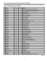
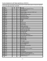
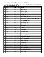
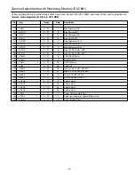
Following adjustments are not required to readjust when replacing the memory IC.

Note: +B (+115V) Voltage Check and Grayscale Adjustment

must be completed before attempting High Voltage Check.

(1) Connect high voltage voltmeter negative lead to 

ground, and c lead to anode of picture tube.

(2) Tune receiver to an active channel and confirm TV is 

operating properly.

(3) Maximize the beam current by adjusting the contrast 

and brightness controls to maximum. Confirm high 
voltage is within 25.5 KV and 26.5 KV at maximum 
beam current. 

(4) Eliminate the beam current by adjusting the contrast 

and brightness controls to minimum. Confirm high 
voltage does not exceed 29 KV at zero beam current. 

If reading is not within range, check horizontal circuit.
No high-voltage adjustment is provided on this chassis.

HIGH VOLTAGE CHECK

12

43

16

1

18

9

14

8

7

1

C641

C631

D610

R636

J657

D631

D686

C636

D687

R635

VR631

L604

R685

C614

D614

D611

R607

D613

D612

T611

01

01-1

L633

J650

R435

T611-H17

T611-H11

L634

L635

L632

D634

C633

R435-H2

R435-H1

C

C502

C503

R510

C509

C

R511

R441

C441

L441

C617

KDY-6

L462-H2

J651

T611-H2

T611-H8

R246

T611-H5

T611-H13

TP-B

R495

R435A

R435A-H1

J649

JP

C442

R445

JW12

JW13

JW14

JW16

T611A-H9

T611A-H13

T611A

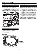
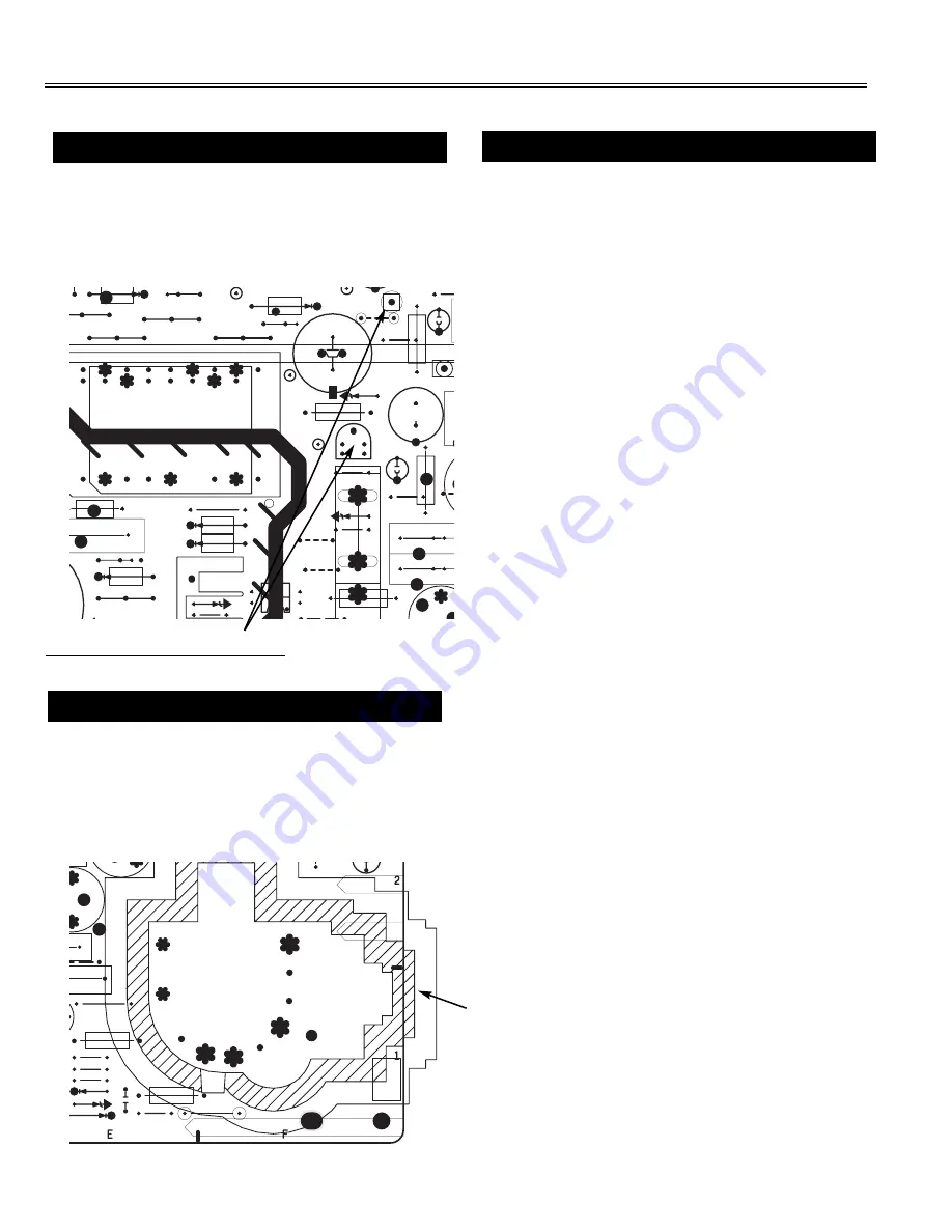
(1) Connect DC meter to TP-B and the ground. 
(2) Tune the receiver to an active channel and synchro-

nized picture. Select NATURAL picture mode by press-
ing the 

PICTURE MODE

button on the remote control.

(3) Adjust B-voltage to be 115 ± 0.5V DC by using VR631. 

B-VOLTAGE SUPPLY CHECKING

(1) Receive the monochrome circular pattern.
(2) Set the brightness to normal and contrast to maximum.
(3) Adjust the focus control on the F.B.T. for the best focus

on the screen centre.

FOCUS ADJUSTMENT

MAIN BOARD

B-Voltage Supply Adjustment

MAIN BOARD

TP-B

R

R424

R474

R482

T471

T471-H2

T471-H4

T471-H10

T471-H1

T471-H7

T471-H5

D465

L461

R466

D353

C355

R355

D469

C

4

R422

L462

R426

R421

C440

J645

L461A

62-H2

62-H1

L463-H1

C440A

Focus VR
(Upper side)

VR631

SM_21-BE4B (FC8-A) IDN  6/24/08  10:53 AM  Page 16

Summary of Contents for CT21KS2

Page 1: ...puts Phono jack L R 1 436mVrms Impedance less than 600Ω Speaker 5 cm 9 cm 2 pcs Sound Output RMS 5W 5W Dimensions 580 W 465 H 326 D mm Weight approx 19 7 Kg Specifications subject to change without notice Original Version Chassis Series FC8 A BE4B FILE NO Model No CT21KS2 Service Ref No CT21KS2 00 Thailand Give complete SERVICE REF NO for parts order or servicing It is shown on the rating plate at...

Page 2: ...without danger of electrical shock X RADIATION PRECAUTION The primary source of X RADIATION in television receiver is the picture tube The picture tube is specially con structed to limit X RADIATION emissions For continued X RADIATION protection the replacement tube must be the same type as the original including suffix letter Excessive high voltage may produce potentially hazardous X RADIATION To...

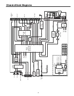
Page 3: ...VD AV OUT D1911 LED DY FBP ABL E W FBP ABL E W L2 IN R2 IN V2 IN AUDIO L AUDIO R L OUT R OUT WOOFER OUT L OUT R OUT V OUT H OUT V OUT HORIZ DRIVE TRANS L1 IN L DVD IN R1 IN R DVD IN V1 IN CR IN CB IN Y IN IF VIF VIF FM OUT L OUT R OUT R OUT G OUT B OUT L2 IN R2 IN 1 5 9 2 15 13 3 14 5 12 1 11 4 1 4 5 34 35 70 57 58 20 49 12 79 37 36 28 ON High OFF Low RC IN KEY IN SW 1 SW 2 10 9 RF AV1 AV2 DVD SW ...

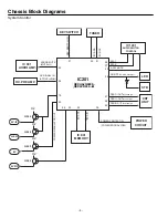
Page 4: ...NTROL CRT UNIT OSD R OUT Active High OSD G OUT Active High OSD B OUT Active High IC 801 MEMORY POWER CIRCUIT POWER PROTECT IN POWER ERROR LOW IIC SCL IIC SDA KEY SWITCH IN 32 36 28 76 50 37 34 35 30 31 45 46 47 29 5V IF 5V DEF 8V 11V 11V 11V Q205 Q206 Q203 POWER REGULATOR OUT IIC SCL IIC SDA 26 40 27 SW 1 SW 2 A SW MUTE 5 VRC Q202 11V 56 QXXAAJQ0897 QXXAVD032 M QXXAAJQ0899 QXXAVD034 M ...

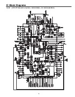
Page 5: ... 5 IC201 CPU IF Video Chroma Def QXXAVD034 M QXXAAJQ0899 IC Block Diagrams ...

Page 6: ...tput amplifier Output amplifier Ripple Filter Ri 30kΩ Ri 30kΩ 2 7 4 5 3 6 9 14 13 11 Vcc ground shorting protection circuit Load shorting protection circuit Thermal protection circuit 10 12 IC501 Vertical Output LA78141 E Thermal Protection AMP Pump Up 1 INVERTING INPUT 2 Vcc 3 PUMP UP OUT 4 GND 5 Ver OUTPUT 6 OUTPUT STAGE Vcc 7 NON INV INPUT ...

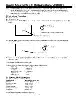
Page 7: ...een The following picture appears on the screen 5 Switch off the TV set by pressing the Power Switch button on the TV set while the above On Screen Display is still on the screen This completes the initialization of memory IC Following shows the initialized contents of memory data by this procedure Plug play No executed Inhibit data Cancelled Ch skip data Cancelled Sound volume data 10 63 steps Vo...

Page 8: ...essing the VOLUME or VOLUME button on the remote control handset Example 1 button POS 1 01 02 03 04 05 200 200 96 95 94 93 01 MENU TV AV CH TIMER x VOLUME VOLUME Display for Align RF AGC Threshold RF AGC adjustment Item No Item Data value FC8 A VER 0 10N NO NAME DATA 91 RFAGC 1AH XX0110101010 1 1101111 2 11111000 Display for V SCO V S Correction adjustment Data value for Red Display for DRV White ...

Page 9: ...T 0 F 5 Align vertical position 16 HBL 0 7 4 Left H Blanking Control 17 V LIN 0 1F 12 Align vertical linearity 18 HBR 0 7 4 Right H Blanking Control 19 V SC 0 1F 14 Align vertical S correction 20 VTEST 0 3 0 Select vertical DAC test mode 21 VCOMP 0 7 7 Align vertical size compensation 22 CDMOD 0 7 0 Select vertical countdown mode 23 VIL T 0 1 0 Vertical deinterlace SW 24 VILT2 0 1 0 Vertical deint...

Page 10: ... 64 AUTOG 0 7 0 Adjust Auto Green level 65 TINT 0 1 0 Set tint center value 66 WBADJ 0 1 0 Auto correct black level 67 IDKIL 0 7 4 Select color ident operational level 68 CVCOA 0 7 4 Control free Run frequency of chroma VCO 69 CVCOC 0 1 0 VCO free run mode 70 FSCSP 0 1 1 Select 10 pin output 71 COLSY 0 7 2 Select Color System 72 RBGAI 0 F A R Y B Y Gain Balance 73 RBANG 0 F 5 R Y B Y Angle 74 RYLE...

Page 11: ...n 109 EWDC 0 3F 18 Align East West DC bias 100 EWAMP 0 3F 0A Align East West amplitude 111 EWTIL 0 3F 20 Align East West Trapezoid 112 EWBOT 0 F 0B Align East West Bottom corner correction 113 EWTOP 0 F 0A Align East West Top corner correction 114 EWCSW 0 1 0 Select control range for Corner correction 115 EWTES 0 1 0 Select East West DAC test mode 116 HSCMP 0 3F 07 Align horizontal size compensati...

Page 12: ...gn sync to fly back phase 60Hz data 156 VSZ60 0 FF 0 Align vertical amplitude 60Hz 157 VDC60 0 FF 0 Align vertical DC bias 60Hz 158 VSF60 0 FF 1D Align vertical position 60Hz 159 VL160 0 FF 0 Align vertical linearity 60Hz 160 VSC60 0 FF 0 Align vertical S correction 60Hz 161 VC060 0 FF 0 Align vertical size compensation 60Hz 162 EWD60 0 FF 1 Align East West DC bias 60Hz 163 EWA60 0 FF 0 Align East...

Page 13: ...FF 0 BRIGHT 60Hz 188 COL60 0 FF EA COLOR 60Hz 189 SUBTT 0 FF 0B SUB TINT 190 SECRY 0 3F 3D Bias R Y DC LEVEL SECAM 191 SECBY 0 3F 3F Bias B Y DC LEVEL SECAM 192 RBANT 0 1F 0 R Y B Y ANGLE NTSC 193 RBAV3 0 1F 5 R Y B Y ANGLE VIDEO 194 VOL G0 0 7F 0 Volume Gain 0 195 VOL G1 0 7F 36 Volume Gain 1 196 VOL G2 0 7F 53 Volume Gain 2 197 VOL G3 0 7F 68 Volume Gain 3 198 POMT 0 7F 17 Power ON Video Mute Ti...

Page 14: ...olour line If line does not appear place this control to maximum fully clockwise 9 Raise each CUT OFF Level with 1 2 3 4 5 and 6 keys to obtain just visible white line 10 Select No 39 WHITE BALANCE Drive Adjustments 11 Adjust Red and Blue Drive Levels alternately with 1 3 4 or 6 key to produce normal black and white picture in highlight areas 12 Check for proper grayscale at all brightness levels ...

Page 15: ...hrome circular pattern 2 Set the brightness and contrast to maximum 3 Select 7 Align Vertical Amplitude in the service mode 4 Change value to be optimum vertical size 5 Exit from service mode Item 7 V SIZE 50 VERTICAL SIZE Horizontal centre Vertical size c Upper Center Bottom d e a b Upper Center Bottom 1 Receive a crosshatch pattern 2 Select a picture mode of NATURAL by pressing the PICTURE MODE ...

Page 16: ...6 J657 D631 D686 C636 D687 R635 VR631 L604 R685 C614 D614 D611 R607 D613 D612 T611 01 01 1 L633 J650 R435 T611 H17 T611 H11 L634 L635 L632 D634 C633 R435 H2 R435 H1 C C502 C503 R510 C509 C R511 R441 C441 L441 C617 KDY 6 L462 H2 J651 T611 H2 T611 H8 R246 T611 H5 T611 H13 TP B R495 R435A R435A H1 J649 JP C442 R445 JW12 JW13 JW14 JW16 T611A H9 T611A H13 T611A 1 Connect DC meter to TP B and the ground...

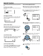
Page 17: ...t position tunes in Select OFF to start from TV mode ON to start from AV1 mode or chan nel number 1 255 to start from it s initial position 4 Start Mode setting TUNING LOCKED How to set the special function Note When making the VOLUME LOCK setting set the desired maximum sound volume by pressing the VOLUME or button before entering Special Function setting mode AV1 MUSIC Turns black screen 4 Press...

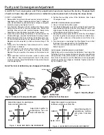
Page 18: ...as controls Readjust the yoke position if necessary until all screens are pure 7 Adjust each Bias control and screen control to obtain white raster Refer to Gray Scale Adjustment If part of the picture screen is coloured adjust the Deflection Yoke position forward or backward slightly 8 Tighten the mounting screw of the Deflection Yoke Adjust Convergence next CENTRE CONVERGENCE ADJUSTMENT 1 Use a ...

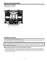
Page 19: ...protective circuit and restore power supply turn the power to the TV set OFF and then ON again via either the main power switch or the ON OFF button on the remote control This will work only if the power supply trouble was temporary If there is permanent trouble such as a damaged circuit power cannot be restored and the circuit will have to be repaired This TV set has a built in power supply prote...

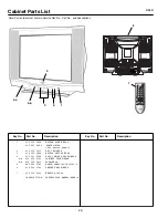
Page 20: ...ND BE4A 3 610 339 2844 BUTTON UNITED BE4A 4 610 341 2368 ASSY CABINET FRONT BE4A 4 a 610 339 2769 CABINET FRONT BE4A 4 b 610 339 2813 DOOR BE4A 5 645 069 2185 BADGE SANYO 43 5X10L43 5 6 610 339 2769 CABINET BACK BE4A 7 652 002 0634 REMOCON JXPSG 1AA6P1P5576 A INSTRUCTION MANUAL BE4B A Key No Part No Description Key No Part No Description 6 Cabinet Parts List BE4B 7 ANT 75 VIDEO AUDIO R L R L VIDEO...

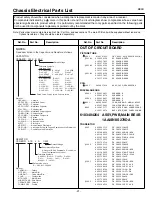
Page 21: ...ny area of a receiver Components indicated by a mark in this parts list and the circuit diagram show components whose value have special significance to product safety It is particularly recommended that only parts specified on the following parts list be used for components replacement pointed out by the mark Note Parts order must contain Service Ref No Part No and descriptions The main PCB unit ...

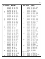
Page 22: ...4051739615 TR 2SA1235A1E 4051739714 TR 2SA1235A1F Q501 4051648412 TR KTC3875S GR RTK 4050144519 TR 2SC2412K T146 R 4050144618 TR 2SC2412K T146 S 4050158724 TR 2SC2812 L6 TB 4050158922 TR 2SC2812 L7 TB 4051631612 TR 2SC2812N L6 TB0 4051739813 TR 2SC3928A1R 4051739912 TR 2SC3928A1S Q631 4051648412 TR KTC3875S GR RTK 4050144519 TR 2SC2412K T146 R 4050144618 TR 2SC2412K T146 S 4050158724 TR 2SC2812 L6...

Page 23: ... 50V 4033670417 CERAMIC 0 1U K 50V 4033053517 CERAMIC 0 1U Z 50V C1008 4041044900 CERAMIC 0 1U K 50V 4040912606 CERAMIC 0 1U K 50V 4033670417 CERAMIC 0 1U K 50V 4033053517 CERAMIC 0 1U Z 50V C1009 4040987901 ELECT 100U M 10V 4040854203 ELECT 100U M 10V 4040971801 ELECT 100U M 16V 4040842804 ELECT 100U M 16V 4040970002 ELECT 100U M 25V 4040892700 ELECT 100U M 25V C101 4040988403 ELECT 470U M 10V 40...

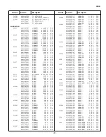
Page 24: ...J 50V 4040947004 CERAMIC 15P J 50V 4031554214 CERAMIC 15P J 50V C225 4032750318 POLYESTER 0 47U J 50V 4032560808 MT COMPO 0 47U J 50V C226 4041046706 CERAMIC 0 047U K 50V 4040914501 CERAMIC 0 047U K 50V C227 4040987901 ELECT 100U M 10V 4040854203 ELECT 100U M 10V C228 4041032907 CERAMIC 0 01U K 50V 4040901204 CERAMIC 0 01U K 50V 4032152211 CERAMIC 0 01U K 50V C229 4031818306 POLYESTER 0 1U J 50V 4...

Page 25: ...27 ELECT 2200U M 25V C510 4041160105 POLYESTER 0 22U J 100 4032889107 POLYESTER 0 22U K 100V 4033407112 MT COMPO 0 22U J 100V C601 4040881704 MT POLYEST 0 22U K 250V 4040888802 MT POLYEST 0 22U M 275V 4040941804 MT POLYEST 0 22U K 275V C602 4040796503 MT POLYEST 0 068U M 250V 4040920700 MT POLYEST 0 068U M 275V 4041144501 MT POLYEST 0 068U K 275V C603 4041078400 CERAMIC 1000P K 1K 4040846307 CERAM...

Page 26: ...12565918 MT GLAZE 2 7K JA 1 10W R1025 4011506110 MT GLAZE 2 2K JA 1 10W R1026 4010269600 CARBON 470 JA 1 6W R1027 4011505816 MT GLAZE 100K JA 1 10W R1028 4010269600 CARBON 470 JA 1 6W R1029 4011505816 MT GLAZE 100K JA 1 10W R103 4012567219 MT GLAZE 18K JA 1 10W R1034 4011505816 MT GLAZE 100K JA 1 10W R1041 4012562917 MT GLAZE 150 JA 1 10W R1042 4011506110 MT GLAZE 2 2K JA 1 10W R105 4012556510 MT ...

Page 27: ...IDE MT 180 JA 2W R601 4010088607 CARBON 220K JA 1 2W R602 4020980106 WIRE WOUND 1 8 KA 7W R603 4010642601 OXIDE MT 0 56 JA 2W R604 4010642601 OXIDE MT 0 56 JA 2W R607 4010169653 CARBON 27 JA 1W R607 4010260409 CARBON 27 JA 1 6W R609 4010246700 CARBON 100 JA 1 6W R610 4010247004 CARBON 1K JA 1 6W R611 4010144056 CARBON 1 5K JA 1 4W R612 4010082605 CARBON 180K JA 1 2W R628 4020008305 SOLID 5 6M KA 1...

Page 28: ...ZJ10B 52 D101 4070996122 ZENER DIODE MTZJ10B 4080472207 ZENER DIODE MTZJ10B 52 D102 4070639108 ZENER DIODE MTZJ6 8B 4080478506 ZENER DIODE MTZJ6 8A D103 4072568911 ZENER DIODE HZS33 2 TA 4071000224 ZENER DIODE MTZJ36A 4070562307 ZENER DIODE RD36EB1 4080476205 ZENER DIODE MTZJ36A D1101 4072505817 ZENER DIODE KDZ10V 4072065618 ZENER DIODE UDZS TE 1710B D1104 4070996122 ZENER DIODE MTZJ10B 4080472207...

Page 29: ...IODE L1SS355T1G 4071630411 DIODE 1SS352 TPH3 4071490817 DIODE 1SS355 TE 17 D801 4072505817 ZENER DIODE KDZ10V 4072065618 ZENER DIODE UDZS TE 1710B D802 4072505817 ZENER DIODE KDZ10V 4072065618 ZENER DIODE UDZS TE 1710B D803 4072505817 ZENER DIODE KDZ10V 4072065618 ZENER DIODE UDZS TE 1710B D804 4070996122 ZENER DIODE MTZJ10B 4080472207 ZENER DIODE MTZJ10B 52 D805 4070996122 ZENER DIODE MTZJ10B 408...

Page 30: ...66800 CERAMIC 1000P K 2K 4032903962 CERAMIC 1000P K 2K C710 4041093106 ELECT 10U M 250V 4034517810 ELECT 10U M 250V RESISTOR R702 4011622711 MT GLAZE 180 JA 1 10W R704 4012559016 MT GLAZE 82 JA 1 10W R705 4011622711 MT GLAZE 180 JA 1 10W R706 4011622711 MT GLAZE 180 JA 1 10W R707 4012559016 MT GLAZE 82 JA 1 10W R711 4010654505 OXIDE MT 12K JA 2W R712 4010654505 OXIDE MT 12K JA 2W R713 4010654505 O...

Page 31: ... C634 C644 D633 C633 C643 R634 R642 JP684 J1103 J1102 J1101 J1100 C007 C010 R013 C006 C009 C005 J015 J009 J014 J246 C223 R232 KP J815 J006 J005 J001 J002 J004 J245 J003 J247 J243 C801 R809 R808 R806 J011 J814 J658 J813 R811 J805 J807 J808 IC801 J810 R645 J660 R690 C691 JP803 Q683 R686 R684 C689 R688 R646 R108 J812 J656 R435 H2 R435 H1 Q461 R462 C470 R426 R427 D421 R421 J108 J404 R440 R504 C506 J65...

Page 32: ...468 R646 H1 R646 H2 L1901 D003 R834 J834 J830 Q432 H2 KG KE KF C628 R603 R604 R613 R612 C465 C467 C440 J645 C441 KDY Q432 1 Q432A 1 Q432 Q432A H2 R508 R509 J403 J503 L441 J1006 J200 J201 J202 J802 J804 J1011 C617 C508 J1012 J203 C1012 C1011 L461A K1002 J007 C1014 J008 T431 K1001 R513 KDY 3 KDY 5 KDY 6 KDY 1 L462 H2 L462 H1 Q432A J651 T611 H2 T611 H8 L441 H2 L441 H1 T431 H3 T431 H2 T431 H1 T431 H4 ...

Page 33: ...CRT Board Parts Side Component Locations X X 1 1 3 5 1AA4B10S0470B K7P K7Y C710 L702 R716 R711 R715 R713 C708 C708A K7U R732 R717 C701 Q703 R712 Q705 Q701 C721 K7Q CAUTION K701L AT FOCUS PIN R B G HIGH VOLTAGE R702 C703 R701 R706 R705 C707 C705 R707 R704 R724 JP741 D741 D742 JP742 R743 R723 Q721 R703 R G B 8V GND 180V HEATER GND CRT Board Solder Side ...

Page 34: ... 5V C 7 9V B 7 7V Q801 E 0V C 7 8V E 0 2V Q886 E 0V C 0V B 0 7V Q802 E 0V C 0V B 0 65V Q683 E 27V C 26 8V B 26 3V Q684 E 0 5V C 0 6V B 1 2V 1000Vp p Horiz 37 4Vp p 3 6Vp p 4 4Vp p 3 67Vp p 3 83Vp p 2 5Vp p 51 67Vp p 11 6Vp p 2800Vp p 4 4Vp p IC201 pin20 Sandcastle IC201 pin19 H drive IC201 pin47 R out IC201 pin46 G out IC201 pin45 B out IC201 pin68 CVBS int IC501 pin5 V out Q432 C H out Q432 B H o...

Page 35: ...s CRT Board Q703 E 2 3V C 9V B 2 1V Q701 E 2 3V C 7 6V B 2V Q705 E 2 3V C 9V B 2V Q701 B B drive Q705 C G out Q701 C B out Q703 C R out Q703 B R drive Q705 B G drive 122Vp p 4 7Vp p 128Vp p 5 1Vp p 5Vp p 134Vp p Q721 E 0 9V C 0V B 0V ...

Page 36: ...SANYO Electric Co Ltd June 08 Printed In Thailand ...

Page 37: ... R1101 16EM10 LBWA C219 1 10GJ1KC R110 470K R487 KK100CBJ C355 ERC05 10B D603 RM11C DDXLBB016 ST2AN30100SV IC501 2 1 EM10LBVD C1004 EM10LBWA EM10MFL 1 10GJ100C R839 KK0 01GQ C217 X D460 1 6NF47K R501 2SJ 0 56C R604 EM1LBVD C691 EM1LBWA EM1MFL 2SC3332S Q431 2SC3332R 1 10GJ75C R1009 X L601 H3 1 2SD4 00E MP Q203 X K1001 1 2 3 4 2400010 T471 H4 1 1 10GJ1KC R1904 2400030 PS601 H3 1 100GK2 2FEA C465 UDZ...

Reviews: